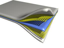
Multi-layered materials are heterostructures composed of many alternating layers that are generally stacked in a periodic manner. An artificially multi-layered material is shown schematically in figure below.

· The combined thickness of two adjacent layers is called the bilayer repeat length or bilayer period.
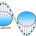
· The principal characteristic of multilayers is a composition modulation, that is, a periodic chemical variation. For this reason, multilayers are often referred to as compositionally modulated materials and the bilayer repeat length is often called the composition modulation wavelength. Many authors prefer to reserve the term ‘compositionally modulated materials’ for multilayers composed of mutually soluble layers separated by compositionally diffuse interfaces.
· Multilayers composed of single-crystal layers that possess the same crystal structure and where the interfaces are in perfect atomic registry are called superlattices.
Properties :
· Fracture: Nano films show enhanced tensile fracture strength compared to fracture strength of micro size films. Polymer multi-layered thin films composed of a high modulus brittle layer and a low modulus ductile layer displayed synergistic improvements in the mechanical properties. These brittle-ductile multilayers have a greater fracture toughness than the brittle material because crakes formed in a brittle layer will be blunted by the adjacent ductile layers.
· Elastic properties: Multi-layered materials show enhanced elastic moduli compared to bilayer materials. Such elastic moduli are called as super modulus effect. This variations in modulus is fairly associated with variations in lattice spacings which can be measured by x-ray diffraction.
· Plastic Properties: Enhancements in the yield strength, ultimate tensile strength and hardness of multi-layered thin film materials. This hardness enhancements are due to interface strengthening effects.
· Damping capacity: Enhancement in the apparent damping capacity of the polycrystalline multi-layered films (Cu-Ni) deposited on fused silica substrates above certain temperatures (300 ˚C). These enhancements may be associated with grain-boundary sliding or with energy dissipation mechanisms localized between the layers.
Synthesis:
· Electrodeposition has proven to be a very successful and relatively inexpensive method of producing high-quality compositionally modulated materials, capable of depositing metallic, ceramic, semiconductor, and polymer multilayers [26,27]. Generally speaking, electrodeposition methods for making multilayers can be divided into two types: alternately plating between two deposition potential using a single electrolyte containing two different types of ion, or periodic transfer of the substrate from one electrolyte to another. In addition to low cost, an attractive feature of electrodeposition is the ability to deposit films over a large area and with a relatively large overall thicknesses (several tens of microns or more), dimensions much greater than those generally associated with vacuum deposition methods. Because of these features, electrodeposition may be the most promising approach with regard to scaling up thin-film processing methods to produce a multi-layered structural material with nanoscale individual layer thicknesses but with a large overall thickness and in-plane area.
· Sputtering has become a very popular preparation technique for the deposition of metallic and ceramic multilayers. Sputtering involves the collisions of ions (usually of an inert gas such as Ar) with the surface of a target material, leading to the ejection of target atoms that are collected in thin-film form onto a substrate. A schematic diagram for an ion gun sputtering system capable of depositing multilayers. An Ar+ ion beam from the target ion gun is used to sputter material from targets mounted on a rotating assembly. Two targets are alternately rotated in and out of the line of the target gun ion beam, resulting in the deposition of a multi-layered film onto a stationary substrate. The substrate ion gun is used to sputter clean the substrate before deposition and can also be used for ion beam assisted deposition processes. Other sputtering systems employ schemes such as alternately
Applications:
· Semiconductor superlattices have important technological applications in the area of high-speed microelectronics ie., in MODFET (modulation doped field-effect transistors)
· In optoelectronic applications, the superlattice photoconductor are those which apply multi-layered materials. Other examples include avalanche photodiodes, infrared lasers, and quantum confined Stark effect optical modulators.