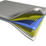
Systems confined in one dimension, or quasi-2D systems, include discs or platelets, ultrathin films on a surface and multi-layered materials; the films themselves could be amorphous, single-crystalline or Nano crystalline.
· A solvent that contains a molecular material that when applied to a surface, chemically aligns itself to form the strongest possible bond and appear as a film. If its thickness is in nanoscale, it is called as Ultra-thin film.
Properties
Thin films are different from bulk materials and they are:
· not fully dense o under stress
· different defect structures from bulk
· quasi – two-dimensional (very thin films)
· strongly influenced by surface and interface effects
· This will change electrical, magnetic, optical, thermal, and mechanical properties. Synthesis methods:
Spin coating or spin casting uses a liquid precursor, or sol-gel precursor deposited onto a smooth, flat substrate which is subsequently spun at a high velocity to centrifugally spread the solution over the substrate. The speed at which the solution is spun, and the viscosity of the sol determine the ultimate thickness of the deposited film. Repeated depositions can be carried out to increase the thickness of films as desired. Thermal treatment is often carried out in order to crystallize the amorphous spin coated film. Such crystalline films can exhibit certain preferred orientations after crystallization on single crystal substrates.
Atomic layer deposition (ALD) uses gaseous precursor to deposit conformal thin films one layer at a time. The process is split up into two half reactions, run in sequence and repeated for each layer, in order to ensure total layer saturation before beginning the next layer. Therefore, one reactant is deposited first, and then the second reactant is deposited, during which a chemical reaction occurs on the substrate, forming the desired composition. As a result of the stepwise, the process is slower than CVD, however it can be run at low temperatures, unlike CVD.
Sputtering relies on a plasma (usually a noble gas, such as argon) to knock material from a “target” a few atoms at a time. The target can be kept at a relatively low temperature, since the process is not one of evaporation, making this one of the most flexible deposition techniques. It is especially useful for compounds or mixtures, where different components would otherwise tend to evaporate at different rates. Note, sputtering’s step coverage is more or less conformal. It is also widely used in the optical media. The manufacturing of all formats of CD, DVD, and BD are done with the help of this technique. It is a fast technique and also it provides a good thickness control. Presently, nitrogen and oxygen gases are also being used in sputtering.
Applications:
Thin film solar cells: Thin-film technologies are also being developed as a means of substantially reducing the cost of solar cells. Thin film solar cells are cheaper to manufacture owing to their reduced material costs, energy costs, handling costs and capital costs. This is especially represented in the use of printed electronics (roll-to-roll) processes. Other thin-film technologies, that are still in an early stage of ongoing research or with limited commercial availability, are often classified as emerging or third generation photovoltaic cells and include, organic, dye-sensitized, and polymer solar cells, as well as quantum dot, copper zinc tin sulphide, Nano-crystal and perovskite solar cells.
Thin-film batteries: Thin-film printing technology is being used to apply solid-state lithium polymers to a variety of substrates to create unique batteries for specialized applications. Thin-film batteries can be deposited directly onto chips or chip packages in any shape or size. Flexible batteries can be made by printing onto plastic, thin metal foil, or paper
Further applications are:
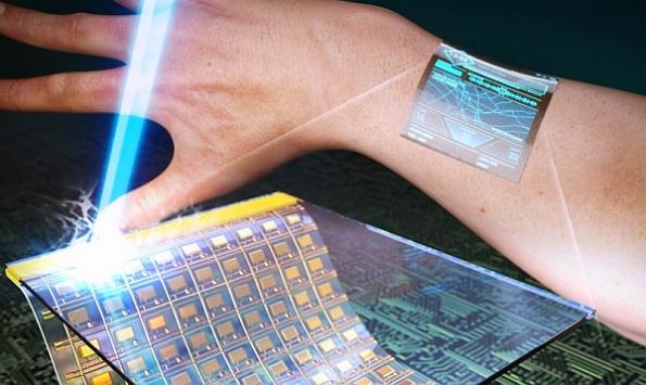
· microelectronics – electrical conductors, electrical barriers, diffusion barriers . . .
· magnetic sensors – sense current (I), Magnetic flux density (B) or changes in them
· gas sensors SAW devices
· tailored materials – layer very thin films to develop materials with new properties
· optics – anti-reflection coatings
· corrosion protection
· wear resistance