There are three categories of materials based on their electrical properties: 1. Conductors, 2. Semiconductors and 3. Insulators. The energy separation between the valence band and the conduction band is called Eg (band gap). The ability to fill the conduction band with electrons and the energy of the band gap determine whether a material is a conductor, a semiconductor or an insulator. In conducting materials like metals the valence band and the conducting band overlap, so the value of Eg is negligible; thermal energy is enough to stimulate electrons to move to the conduction band. In semiconductors, the band gap is a few eV. If an applied voltage exceeds the band gap energy, electron jump from the valence band to the conduction band, thereby forming electron-hole pairs called excitons. Insulators have large band gaps that require an enormous amount of voltage to overcome the threshold. This is why these materials do not conduct electricity. Quantum confinement of materials will change properties of all these materials;

Fig. Schematic illustration of the Eg in insulator, semiconductor and conductor
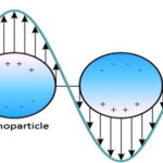
· Bandgap: Quantum confinement is responsible for the increase of energy difference between energy states and band gap as shown in fig. below. Also, at very small dimensions when the energy levels are quantified, the band overlap present in metals disappears and is actually transformed into a bandgap. This explains why some metals become semiconductors as their size is decreased.
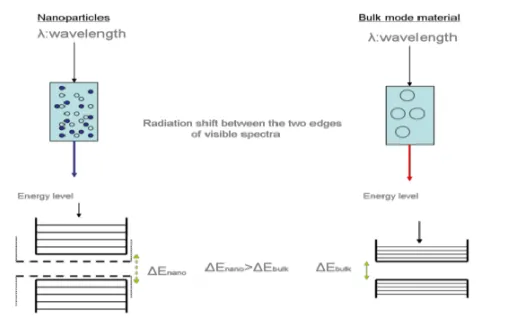
· Absorption and emission in low wavelength: The increase of bandgap energy due to quantum confinement means that more energy will be needed in order to be absorbed by the bandgap of the material. Higher energy means shorter wavelength (blue shift). The same applies for the wavelength of the fluorescent light emitted from the nano-sized material, which will be higher, so the same blue shift will occur. This thus gives a method of tuning the optical absorption and emission properties of a nano-sized semiconductor over a range of wavelengths by controlling its crystallite size.
· Electrical conductivity: Some nanomaterials exhibit electrical properties that are absolutely exceptional. Their electrical properties are related to their unique structure. Two of these are fullerenes and carbon nanotubes. For instance, carbon nanotubes can be conductors or semi-conductors depending on their nanostructure. Nanoparticles made of semiconducting materials Germanium , Silicon are not Semiconductors.
· Nanotubes are long, thin cylinders of carbon and are 100 times stronger than steel, very flexible, and it can be either conducting or semi-conducting based on its diameter, twist and number of walls in the nanotube.
· Negligible resistance: Supercapacitors, which are materials in which there is effectively no resistance and which disobey the classic Ohmś law.
· Ionization potential: Ionization potential at Nano sizes are higher than that for the bulk materials
· Computing power: Nanoelectronics have converted Gigantic computers to handheld computer devices. The very first computers were highly inefficient and took up incredible amounts of space. But nanoelectronics have made computers to be fit in our hand. Many handheld devices have more computing power than the earlier large computers.
· Quantum effects in Nanoelectronics: Counting single electrons: From the development of the first transistor in 1947, great interest has been directed towards the technological development of semiconducting devices and the investigation of their physical properties. A very vital field within this topic focuses on the electrical transport through lowdimensional structures, where the quantum confinement of charge carriers leads to the observation of a variety of phenomena. In the aim of reaching even smaller sized and more compact devices, semiconductor Indium Arsenide nanowires grown via Molecular Beam Epitaxy technique are processed adding source and drain contacts and several types of electrostatically coupled gates. The flexibility in tailoring the chemistry of nanowires will most likely make them the building blocks of nanosized devices.

Figure: Scanning electron microscope image of the molecular-beam-epitaxy grown Indium Arsenide nanowire with electrostatically coupled lateral gates
· One reason to shrink electronic circuits and storage media in size is that integrated circuits also become faster and consume less energy. Storage devices with a high density can be faster accessible. This is a continuing motivation to go from micro to nanoelectronics.
· One driving force for nanoscience and –technology was the desire to miniaturize electric circuits and storage media. Over the past decades, the MOSFET, one standard transistor, has continually been scaled down in size; modern integrated circuits incorporate MOSFETs with feature sizes down to 32 nm. At the same time the size to store one bit of information has decreased to 200 GB/sq.inch leading to bit sizes of 56 nm.