SEMICONDUCTING NANOWIRES
Based on the geometry, 1D nanostructures typically consist of four categories: nanowire (NW), nanorod (NR), nanobelt (NB), and nanotube. The first three categories all possess a solid structure, while the nanotube has a hollow center. There is a significant different in geometry, property, and synthesis strategies between the nanotube and the first three categories, i.e., NW, NR, and NB. In general, NRs are NWs with a small aspect ratio (i.e., short NWs), which typically appear rigid and straight. NB is a special NW structure with a rectangular cross-section. Typical NB structures are single crystals with well-defined side crystal facets. Sometimes, nanofibers were also used to describe the NW morphology, particularly when the NWs are very long and not single crystalline [1]. Nanoscaled materials are of great interest for their unique structure and properties. Compared to isotropic nanoparticles and two dimensional thin films, one dimensional nanostructures such as nanofibers and nanowires are much more anisotropic, i.e., the aspect ratio of length to diameter can attain very high values.
Semiconductor one-dimensional structures, i.e., nanorods and nanowires with diameters ranging from 1 to 400 nm and lengths of up to hundreds of micrometers, are known to have many interesting physical properties and great potential applications in semiconductor and electronic technologies, which have stimulated intensive, worldwide research activities. They are perhaps the most versatile building blocks for optical and (opto-)electronic circuits at the nanoscale. Preliminary studies of some of these one-dimensional nanostructures indicate that they may be used as microscopic probes, field emission sources, storage materials, and light-emitting devices with extremely low power consumption. Among these semiconductors, some metal oxides, for instance, stannic oxide, titanium oxide, cuprous oxide, and vanadium pentoxide are the most important base materials in industry for gas sensors, transistors, and electrode material as well as catalysts. There has been extensive research into various “top-down” and “bottom-up” methods to create these nanostructures. In order to investigate their properties, many methods have been developed to synthesize one-dimensional nanomaterials, such as carbon nanotubes confined chemical reaction, Chemical Vapor Deposition (CVD), Molecular Beam Epitaxy (MBE), vapor-liquid-solid (VLS), solution–liquid–solid (SLS), and template-based synthetic approaches. However, complicated apparatus, complex process control, and special condition may be required for these approaches [2, 3]. Here we will describe VLS method in details.
TITANIUM DIOXIDE (TIO2)
Based on the geometry, 1D nanostructures typically consist of four categories: nanowire (NW), nanorod (NR), nanobelt (NB), and nanotube. The first three categories all possess a solid structure, while the nanotube has a hollow center. There is a significant difference in geometry, property, and synthesis strategies between the nanotube and the first three types, i.e., NW, NR, and NB. Generally, NRs are NWs with a small aspect ratio (short NWs), which typically become rigid and straight. NB is a special NW structure with a rectangular cross- section. Typical NB structures are single crystals with well-defined side crystal facets. Sometimes, nanofibers were also used to explain the NW morphology, particularly when the NWs are very long and not single crystalline.
Since Fujishima and Honda (1972) reported that n-type titanium dioxide (TiO2) could be used as a photo anode for a photo electrochemical cell, titanium oxide has been comprehensively investigated owing to its great applications in many fields [4].
TiO2 naturally exhibits four different types of polymorphs, i.e., rutile, anatase, brookite, and TiO2 (B). In addition, several metastable polymorphs, such as TiO2 (H), TiO2 II, and perovskite, have been produced synthetically. Different phases have different properties and thus require different conditions to form desired morphologies and offer different performance. In general, rutile is the most stable phase, while the anatase, brookite, and TiO2 (B) are metastable and will transform into rutile under high temperature. This phase stability relationship also exists in TiO2 nanomaterial formations. Anatase phased nanomaterials were commonly obtained but always found in solution-based or low-temperature vapor deposition systems. High- temperature deposition or annealing would usually yield rutile TiO2nanostructures. Brookite and TiO2 (B) phases were less common and typically obtained from solution-based growth systems. Other metastable phases have to be synthesized using particular types of precursors and under restrict conditions. They were very rarely observed as a stable nanomaterial phase [1, 5, 6].
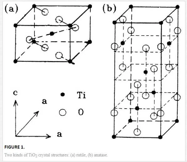
Indeed among the semiconductor oxides, titanium oxide (TiO2) has received more attention during the last decade because of its high refractive index (2.5), high band gap (3 eV), transparency throughout the visible and infrared region, high chemical stability, and hardness [7]. Crystal structures of the two most important phases are anatase (a = 3.78 Å, c = 9.51 Å; space group of I41/amd) and rutile (a = 4.59, c = 2.96, space group of P42/mnm). Each cell of rutile consists of two TiO2 molecules, while anatase has four TiO2 molecules. Figure 1 gives crystal structures of rutile (a) and anatase (b). The common features for these structures are as follows: Ti atom is positioned at the center of six O atoms, forming a deformed Ti-O octahedron. The octahedral share top points and a rhombic side join together and thus construct a crystal. The differences between them exist: three sides shared for the brookite, four for anatase and two for rutile. Among them rutile is the most stable and anatase is less while brookite is not stable. Therefore, the first two are commonly concerned in nanomaterials [4].
TiO2 has showed a wide range of applications in hydrogen production, lithium-ion batteries, fuel cells, gas sensors, detoxification, photovoltaics, photocatalysts, and super capacitors due to its excellent solid-state physical properties [8]. Over the past two decades, there have been remarkable advances in the expansion of one-dimensional (1D) nanostructures. The wire-like structure not only introduces significant enlarged and well-defined crystal surfaces over planar structures but also provides 1D confined channel, which could basically tailor the transportation of electrons, phonons, and photons [9]. The one-dimensional structure such as TiO2 nanowire is considered as a good candidate for getting higher performance in those applications compared to the bulk one. For example, a TiO2 nanowire based electrode can provide a large surface area for effectively collecting photons and electrons [8]. Tao et al. [10] used TiO2 NW array as photo anodes of back-illuminated dye-sensitized solar cells. Shi et al. [11] grew TiO2 nanorods uniformly on dense Si NW array backbones, by using surface-reaction-limited pulsed chemical vapor deposition technique. They developed a 3D high-density heterogeneous NW architecture, which is useful for photo electrochemical electrodes. Wang et al. [12] reported hydrogen-treated TiO2 NW arrays for photo electrochemical water splitting. Mandal and Bhattacharyya [13] presented through systematic studies the performance of TiO2 NWs in sensing, quantification, and photocatalytic degradation of cationic dyes in aqueous solution. Wang et al. [14] indicated that TiO2NWs have promising application for high energy density lithium-ion batteries. Xi et al. [15] grew single-crystalline rutile TiO2 nanorods on fluorine doped tin oxide glass for organic–inorganic hybrid solar cells by means of hydrothermal mechanisms.
Numerous routes have been explored to the synthesis of 1D TiO2 nanostructures from both bottom up and top down. Representative bottom-up approaches include a large variety of solution- and vapor-based growth strategies. Although bottom-up approaches remain as the major synthesis efforts, several top-down procedures have also been explored for 1D TiO2 growth, such as direct oxidation and electrochemical etching techniques. In general, there are four main approaches, which include solution-based synthetic approaches (such as hydrothermal/ solvothermal and sol-gel methods), vapor-based approaches (chemical/physical vapor deposition, atomic layer deposition-related methods and pulsed laser deposition), templated growth, and top-down fabrication techniques. Solution-based growth techniques offer several major advantages for mass production of nanomaterials including low-cost, simple processing, and good scalability. Vapor deposition is typically conducted in vacuum and under high temperature. Compared to the wet chemistry methods, it offers several unique advantages. First, the high quality of NW’s crystallinity is secured due to the utilization of high-temperature and high-vacuum deposition conditions. Second, since the vapor deposition processes are typically performed in conventional thin film deposition systems, the knowledge of thin film growth techniques can be adopted to understanding the NW growth behaviors. Lastly, by engineering catalysts, growth sites, or precursors, the control of location, composition, dimension, and organization of NWs could be achieved via vapor deposition processes. Nevertheless, vapor deposition is usually associated with high cost and small- scale production. Template growth is a very versatile synthesis technique that forms nanostructure with a morphology that follows the porous template. Top-down fabrication techniques describe the creation of nanostructures from the bulk form. This approach typically is able to process a large quantity of nanostructures with uniform morphology and orientation. For TiO2 1D nanostructures, a top-down process usually starts from a bulk Ti foil followed by selective etching and/or oxidization. In the following section, the vapor- liquid- solid mechanism is described [1].
VLS MECHANISM OF NANOWIRE GROWTH
Nanowires are commonly grown using vapor, solution or (template directed) electrodeposition methods. High- temperature growth from the vapor phase is often preferred due to the high crystal quality that can be obtained and the ability to grow large quantities of wires at once. A key factor in most vapor- and solution-based methods is the presence of small metal droplets during synthesis. Analysis of the growth of silicon whiskers (hairs) from the vapor phase using gold catalyst particles leads to the postulation of the vapor- liquid- solid (VLS) mechanism of growth. The VLS mechanism consists of three stages which are illustrated in figure 2A. First, a metal particle absorbs semiconductor material and forms an alloy. In this step, the volume of the particle increases and the particle often transition from a solid to a liquid state. Second, the alloy particle absorbs more semiconductor material until it is saturated. The saturated alloy droplet becomes in equilibrium with the solid phase of the semiconductor and nucleation occurs (i.e., solute/solid phase transition). During the final phase, a steady state is formed in which a semiconductor crystal grows at the solid/liquid interface. The precipitated semiconductor material grows as a wire because it is energetically more favorable than extension of the solid- liquid interface. The semiconductor material is precipitated at the existing solid/liquid interface as opposed to the formation of a new interface.
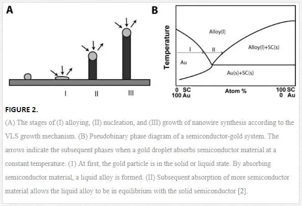
In the VLS mechanism, the wire diameter is determined by the diameter of the alloy particle which is in turn determined by the low temperature size of the metal particle and the temperature. The wire length is determined by the growth rate and time. When the system is cooled, the alloy droplet solidifies at the wire tip. To examine the feasibility of VLS wire growth from a certain semiconductor/metal combination, it is essential to study the (pseudo)binary phase diagram (figure 2B); the metal should form an alloy with the semiconductor at a temperature that also allows the semiconductor to exist in the solid phase. The validity of the VLS mechanism of wire growth has been proven for germanium nanowires by in- situ high- temperature TEM measurements. Heating neighboring gold and germanium clusters to growth temperatures and selectively evaporating the germanium clusters with an electron beam are allowed for the direct imaging of the successive steps of alloying and melting, nucleation and wire growth. A study using colloidal gold catalyst particles showed that using the VLS method, (single) crystalline nanowires with diameters as small as 5 nm could be obtained. In addition, it has been shown that by increasing the VLS growth rate by modulating the temperature, crystallization only takes place at the surface of the catalyst particle resulting in the growth of nanotubes. Since the late 1990’s, semiconductor nanowire growth using the VLS method has enjoyed an increasing popularity with researchers and industry [2]. Some of studies on TiO2 nanowires are listed in Table 1.
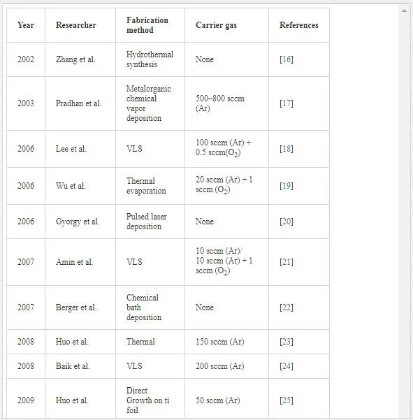
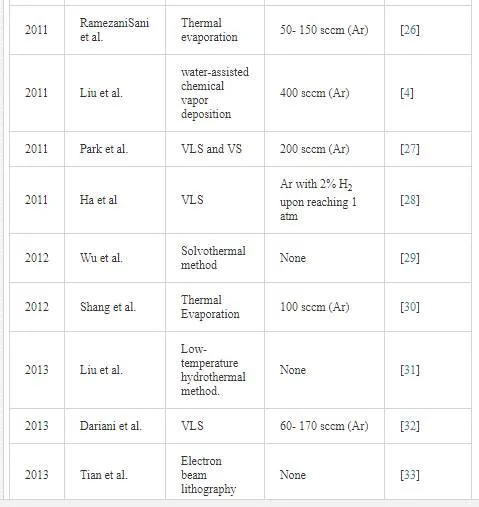
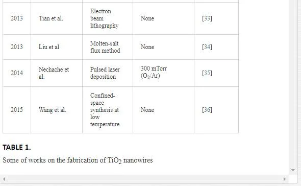
The vapor–liquid–solid and the vapor–solid growth mechanisms have been used to fabricate high-quality oxide NWs with short heating times. Ha et al. [28] synthesized single-crystalline rutile TiO2NWs by VLS method on Ti foil substrates patterned with catalytic Sn nano-islands, Lee et al. [18] grew TiO2 NWs in this way but used Au as catalysts, and Park and Lee [27] reported synthesis of TiO2 NWs by Ni as catalysts.
TiO2 nanowire is typically achieved using either of the two different synthetic methods developed over the past few years: one is the wet-chemistry method such as electrochemical, sol-gel electrophoresis, hydrothermal growth on Ti substrates at 180 ℃ utilizing various organic solvents to oxidize Ti [37], direct oxidizing Ti substrate with aqueous hydrogen peroxide solutions [10], and solvothermal method [38]. The other is the dry method such as, growth single-crystalline TiO2 nanowires by thermal evaporation in atmospheric-pressure (101325 Pa) [30], metal-organic chemical vapor deposition [39], pulsed chemical vapor deposition [8], chemical vapor transport process by evaporating Ti metal powders [18], heating titanium grids (substrate) by ethanol-embedding followed by an annealing in the air [40], and by a facile water- assisted chemical vapor deposition method based on commercial metal titanium [4]. TiO2 nanowires produced by the wet-chemistry method due to poor crystallinity have difficulty integrating into device fabrication. Also, they need additional processes in order to improve their crystallinity [27].
In this work, TiO2 nanowires were synthesized by a carbothermal evaporation process on quartz substrate at 850 ℃ for 1 h at atmospheric pressure (101325 Pa), and Au was used as a catalyst. Also, the influence of argon flow as carrier gas on microstructural and optical characteristics was measured. We have been characterized some microstructural parameters like crystallite size, microstrain within the crystallite, dislocation density, and texture coefficient by the diffraction pattern.
Experimental details
In this study, pieces of quartz with dimensions of 1 × 15 × 15 mm3 are used. Initially, the substrates were ultrasonically cleaned with acetone and ethanol for 10 minutes, respectively. Then a layer of titanium was deposited on substrates by electron beam evaporation technique with the evaporation rate of 0.2 Å/s under the pressure of 1.5 × 10 -5 mbar. In this step, voltage and current were kept 4 kV and 100 mA, respectively. The electron beam evaporation device is specified by: HIND HIGH VACUUM CO. Model 12A4D. After removing the samples, a gold thin layer with 3 nm thickness was coated on the titanium layer by sputtering method.
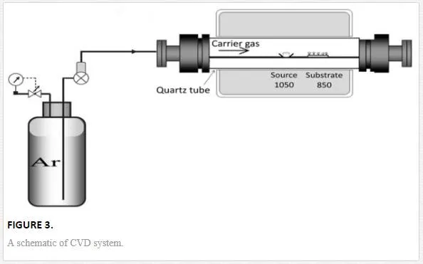
In next step, a tablet containing of titanium and graphite with the ratio of 1:1 as a source material was placed in the center of horizontal furnace. The center of the furnace was heated to 1050℃ with heating rate of 20℃/min. According to phase diagram of the Au-Ti system, the eutectoid temperature is about 832℃ [30]. The eutectoid temperature is a point in which two metals in solid phase form an alloy in solid phase (no in liquid phase). Thus, the sample was placed in distance of 12 – 13 cm (with about 850 ℃ temperature) from the center of the furnace for 1 h at atmospheric pressure and under argon flow. The vapor was generated from source material transported to the substrate and at last condensed on the surface of substrate (see figure 3). Then the substrate was naturally cooled down to room temperature. In this study, three samples under different argon gas flows (60 sccm, 110 sccm, and 170 sccm) were fabricated. Argon gas was also used to control the oxygen content of experiment. It is believed that oxygen comes from leaked air during heating process. Content of argon was kept constant during heating process by using bubbling trap at the end of the vent line. The microstructure and the morphology of the samples were analyzed by x-ray diffraction (XRD: Philips X-Pert PW 3040/60, λ(Cukα) = 1.54 ˚A) and field emission scanning electron microscope (FESEM: Hitachi S4160 with operating voltage of 15 kV), respectively. The absorption spectrum of TiO2 nanostructures was evaluated by spectrophotometer (Ocean Optics, Model HR4000 CG-UV-NIR).
Results and discussion
SEM OBSERVATIONS
The morphologic characteristics of the samples under different carrier gas flows are determined by SEM images. The cross-sectional views of the samples are shown in figure 4.
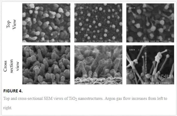
The average range of length and diameter of nanowires are given in Table 2. It can be seen that nanowires become thinner and longer with increasing the carrier gas flow. Since fabrication parameters except argon flow were fixed, it can be concluded that the amount of O2 inside the reaction chamber plays a vital role in the growth of TiO2 1D nanostructures. When the O2 concentration was high, i.e., Ar flow was low, the VLS growth (will describe later) was suppressed because Ti vapor could readily react with O2 before forming alloy droplets with Au as catalyst [12]. Therefore, in this condition, a relatively low concentration of O2 is necessary [13].
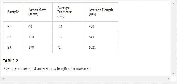
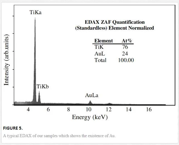
Figure 5 shows compositional energy-dispersive X-ray spectroscopy (EDAX) analysis of the NW tip and the confirmation of the existence of Au alloy.
XRD STUDIES
To examine the effect of argon flow on structural properties of TiO2 1D nanostructure, the XRD analyses were performed. Figure 6 shows XRD patterns of TiO2 grown on Ti/quartz substrates.
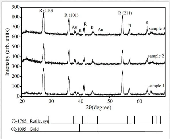
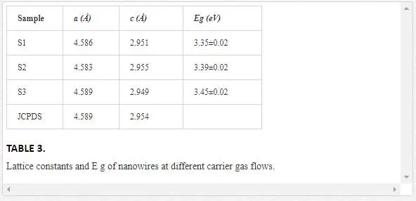
Rutile phase is formed on the samples and (110) direction is preferred direction which is consistent with SEM images. In the TiO2 tetragonal structure, the plane spacing (d) is related to lattice constants (a and c) and the Miller indices (h, k, and l) by the following relation [42]:

The results are presented in Table 3 and are consistent with standard card of JCPDS (73-1765).
OPTICAL PROPERTIES
The absorbance spectrum of TiO2 nanowires is measured by spectrophotometer. According to Beer-Lambert’s law (Eq. 2), transmittance (Eq. 3), and absorbance (Eq. 4) definitions [43], the absorption coefficients of samples according to absorbance are obtained by Eq. 5:
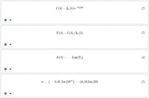
where d is the thickness of samples derived from the cross-sectional images of SEM and A is the absorbance of samples.
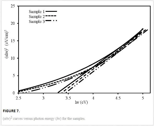
It is known that the relationship between absorption coefficient α near the absorption edge and the optical band gap Eg is determined by Tauc relation [15]:

where C is a constant, n is equal to 0.5 or 2 for direct and indirect allowed transitions, respectively, and hν is photon energy. The Eg can be graphically estimated by a linear fit of the high- energy tail of (αhν)1/n. Since the samples have rutile structure, rutile titania has direct band gap (n = 0.5).Figure 7 shows (αhν)2 plots versus photon energy hν for direct transition and intercepts value of the linear-fit extrapolations with the horizontal axes. The values of Eg are given in Table 2.
The optical results have shown that all the samples are characterized by energy gap higher than bulk rutile TiO2 (Eg = 3 eV for bulk) [28]. As the carrier gas concentration increases, the band gap increases from 3.35 to 3.45 eV. The higher value of the rutile titania energy gap are attributable to the well-known relationship between band gap and crystallites size. The appearance of quantum confinement effect in small sized nano crystalline titania is resulting in a blue shift of the band gap [37]. Among the samples, sample 3 has the highest Eg value which is the thinnest one.
GROWTH MECHANISM
One-dimensional nanostructures are grown in this study by VLS mechanism. In the mechanism, the role of the impurity (catalyst) is to form a liquid alloy droplet of eutectoid temperature. Metal catalyst used in the mechanism was gold with 3 nm thickness. At high temperatures (about 850℃) alloy liquid droplets of Au-titanium form. On the other hand, during the thermal evaporation process, at first, titanium powder in the presence of oxygen atmosphere was converted toTiO2 powder (see Eq. 7) [44], then the TiO2 powder was reduced by graphite to produce Ti vapor as the following chemical reaction [45].

We have used Ti metal and carbon instead of TiO2 in carbothermal reduction process. In fact, Ti in the tablet converts to TiO2 by oxygen in air (Eq. 7), and then TiO2 is reduced in carbothermal reduction process by carbon (Eq. 8). Indeed, carbon mainly was used for TiO2 reduction. Also there are some papers that have used titanium and carbon as a source material [26, 46]. Previously, TiO2 and C as a source material were examined in our lab but NWs did not grow. Amin et al. [21] also reported that continuous increase of the amount of oxygen further reduced the yield of TiO2 1D nanostructures. When the O2 concentration was high, the VLS growth was suppressed because Ti vapor could readily react with O2 before forming alloy droplets with catalytic materials.
Since the adsorption of liquid is more than solid, the reactant components (vapor of titanium and oxygen) absorbed into the alloy. The liquid alloy acts as a preferred sink for arriving nanostructure components. The Ti and O2 are dissolved into the mediating alloy liquid droplets. When alloy droplets reach to saturation of reactive component, the 1D nanostructures grow by precipitation of TiO2 from the droplets in the interface liquid- solid to minimize free energy of alloy system. The 1D nanostructure grows in length by the mechanism until the Au is consumed or until the growth conditions are changed [47]. Here, by over an hour, furnace temperature began to reduce and growth condition of one-dimensional titanium dioxide nanostructures is stopped.Usually droplets of catalyst are observed on the top of the nanostructures in a VLS- based growth system. However, the position of catalyst at the tip or root of the nanostructure depends on the interaction of catalyst nanoparticles and the substrate [48].SEM images (Figure 4) show by increasing argon flow or decreasing oxygen (one of reactants), nanowires become thinner and longer. O2 plays a main role in the growth of TiO2 nanowires. When O2concentration is high, i.e., Ar flow is low, Ti vapor could readily react with O2, before they adsorb on alloy droplets [30]. Therefore, in this condition, a relatively low concentration of O2 is necessary [15, 31]. According to other findings [17, 27, 48], we suggest that thinner and longer NWs with increasing Ar flow are due to the following reasons:
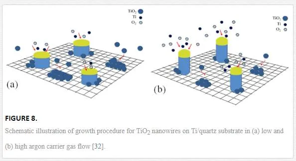
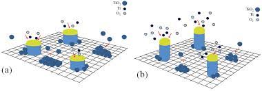
Argon flux plays a major role in combining Ti and O2 and producing TiO2. A schematic of the proposed growth mechanism is shown in Figure 8. When Ar flux is low (Figure 8a), the possibility of producing TiO2 is much higher than when Ar flux is high (Figure 8b). The reason could be due to moving Ti and O2 gases from furnace tube when Ar flux is high and so the possibility of producing TiO2 becomes lower. On the other hand, in presence of O2, titanium layer on the substrate surface in 850℃ is easily converted to TiO2 (according to XRD diffraction patterns and Eq. 7). Thus, there is a competitive growth between TiO2 layer (epitaxial growth: TiO2 molecules on TiO2 layer) and alloy droplets (VLS growth). TiO2 islands that are formed around the NWs by VLS method become larger with decreasing Ar flow. Since the other parameters of growth, such as source and time are constant, NW diameters and lengths become larger and shorter, respectively.Moreover, TiO2 is heavier than Ti and O2, so probably exists in lower height than them. Therefore, TiO2 can be absorbed into the nanostructure bodies more likely than their tips (alloy droplets), to be absorbed, so when TiO2 is more than Ti and O2, nanostructures will be shorter and thicker. Therefore, with increasing Ar gas flow, the crystallinity improves due to VLS growth method.RamezaniSani et al. [26] have grown TiO2 nanowires by thermal evaporation on a silicon substrate with the major reflection along (101) direction. Their results indicate that a convenient gas flow for controlling diameter size of nanowires is about 100 sccm, While our substrate is quartz and the major reflection growth along is (110) direction. Also we see that with increasing gas flow from 60 to 170 sccm, nanowires become thinner and longer.
MICROSTRUCTURE CHARACTERIZATION (THEORETICAL BACKGROUND)
Deviation from the ideal crystallinity such as finite crystallite size, strain (at the atomic level), and extended defects (stacking faults and dislocations) leads to broadening of the diffraction lines. Crystallite size is a measure of the size of coherently diffracting domains and is not generally the same as particle size due to polycrystalline aggregates. Strain is defined as change in length per unit length and is measured as the change in d spacing of a strained sample compared to the unstrained state [49].
According to Scherrer [50], the apparent crystallite size can be obtained as follows:

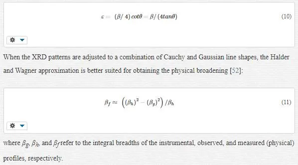
where K is a constant close to unity, θ is the Bragg angle of the (hkl) reflection, and λ is the wavelength of X-rays used. DV is a volume-weighted quantity. Wilson in 1963 used integral breadth β instead of FWHM in Eq. (9).The dependence of strain ε to line broadening is defined as follows [51]:
THE WILLIAMSON–HALL INTEGRAL BREADTH METHOD
Williamson and Hall in 1953 proposed a method for resolving size and strain broadening. Williamson–Hall plots can be applied to a Gaussian profile as follows [53]:

A plot of (βf*)2 against 4d*2 gives a straight line. From the intercept and slope of line size, strain can be calculated.
MICROSTRUCTURE STUDY IN TIO2 NANOWIRES
X-ray diffraction (XRD), in which strong scattered intensity is observed at specific angles of scattering, has been widely used for decades in the determination of structural and microstructural parameters. By the diffraction pattern, we have characterized some microstructural parameters like crystallite size, microstrain within the grain, dislocation density, and texture coefficient.
THE WILLIAMSON–HALL INTEGRAL BREADTH METHOD
From an analysis of XRD line broadening, the contributions due to crystallite size and lattice strain can be determined. Here, crystallite size and microstrain contributions are separated using the Williamson–Hall (W-H) method. Assuming contribution to the Bragg peak having both Lorentz and Gauss profile [54]:

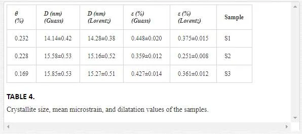
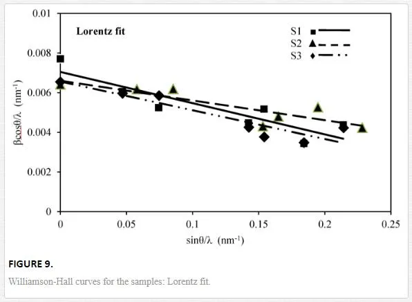
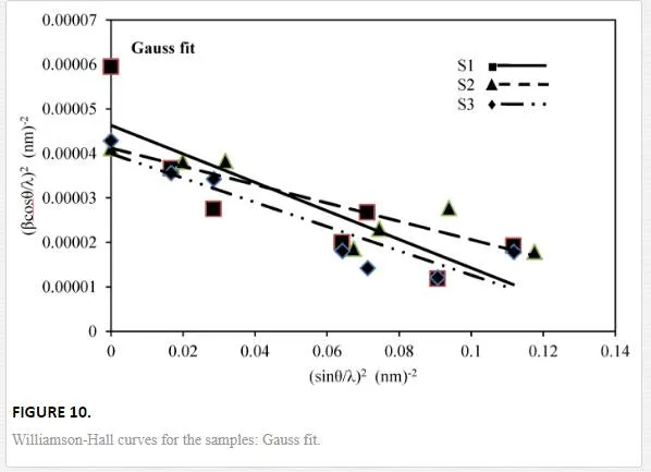
By plotting βcosθ/λ vs sinθ/λ (Lorentz) or (βcosθ/λ)2 vs (sinθ/λ)2 (Gauss), one can estimate the microstrain from the line slope and inverse of the crystallite size from its y-intercept. Figures 9 and 10indicate W-H curves for the samples in Lorentz and Gauss fits, respectively. The obtained values from W-H curves are given in Table 4. The plotted W-H curves indicate that strain and size contributions exist simultaneously in the samples.
DILATATION
Volume strain or dilatation is a change in volume that defines as [55]:

The calculated dilatations are given in Table 4. The slopes of the W-H curve for the samples are negative, i.e., their strain is negative and there is a contraction of epilayer on substrates which means compressive stress. The different slopes represent different mean microstrains.
It is well known that strain has direct relation with elastic energy [55]. Evaporated particles from source due to their temperature have certain kinetic energy. In low Ar flow (60 sccm), Ar particles is lower than evaporated particles then collision between them is negligible. However, with increasing Ar flow to 110 sccm, collision between Ar particles and evaporated particles increases therefore it could have reduced the evaporated particles energies and microstrain. However, with increasing Ar flow up to 170 sccm, the number of Ar particles enhanced compared to evaporated particles, so they can help to increase the evaporated particles movement. Therefore, their velocity and energy increase and also mircostrain increases.Both dilatation and microsrain are negative and at the same order. We compare these two quantities, because the microstrain (obtained from W-H curve) is average of strain in volume not in specific direction. Thus, calculated strain from main definition must consider in volume.We can compare volume strain (which found from lattice parameters) and microstrain (which found from XRD pattern) because the microstrain from the W-H curve does not have any particular direction. By comparing them, it reveals that they have approximately good agreement both in magnitude and sign.
DISLOCATION DENSITY
To estimate the dislocation density, ρD (dislocation density due to domain size), ρε (dislocation density due to strain) and ρ (real dislocation density), the simple approach of Williamson and Smallman (1956) is followed, relating ρ to crystallite size D and strain <ε2>1/2 [58]:
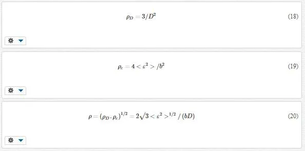
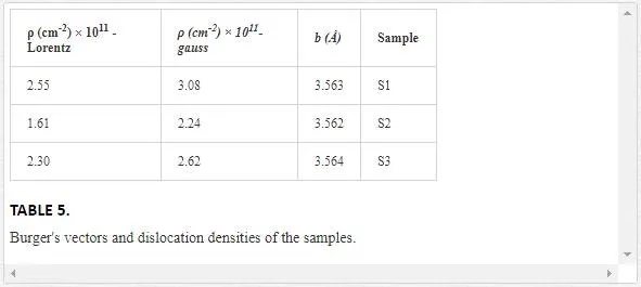
where b is the Burger’s vector, which determines distance and direction of displacement. We assumed that the magnitude of Burger’s vector is calculated by [(a2/4)+(a2/4)+(c2/4)]1/2, where a and c are lattice parameters. Dislocation densities in actual crystals depend on the preparation of the specimen, but can range from 102 to 1012 cm-2 [59], and the dislocation values of our samples are in the same range
(Table 5).According to Eq. 16, behavior of dislocation density is similar to microstrain, i.e., the value of dislocation density decreases from sample S1 to S2, 4and then increases from S2 to S3, since dislocation density and microstrain are related to displacement. It is noted that the results of Lorentz and Gauss fits for our samples are the same.
TEXTURE COEFFICIENT
In order to clearly understand the preferred orientation of the samples, the texture coefficient TC(hkl) of each XRD pattern is calculated according to the following formula [60]

where I(hkl) is measured intensity of the (hkl) diffraction peak and N is the amount of crystal directions which is 11, 10, and 12 for samples 1, 2, and 3, respectively. If TC(hkl) equals to 1, there is no preferred orientation on (hkl) direction of the film. When this value is larger than 1, a preferred orientation exists along the (hkl) plane. The standard deviation TC(hkl) of the TC values from powder condition is [60]:

If σ equals to zero, the crystallite orientation of a film sample is the same as that of the related powder-shaped sample and there is no preferred direction. Therefore, σ value indicates the preferred orientation level of thin film samples [61]. The values of texture coefficient and its standard deviation for the samples are shown in Table 6. As expected, the preferred direction in the samples is (110). It is concluded that the different carrier gas flows do not influence the preferential orientation. The rutile (110) surface is the most stable crystal face and has lowest surface energy [62]. According to Table 6, the behavior of TC (110) is similar to dislocation density, i.e., dislocation helps the growth of (110) plane, which is the most stable plane in the rutile phase.
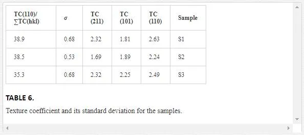
In order to better determine the contribution of TC (110) to other TC (hkl), the proportion of its value to total value of all TC(hkl) was calculated, (i.e., TC(110)/∑TC(hkl)). The values obtained for samples 1, 2 and, 3 were 38.9, 38.5, and 35.3, respectively. It is observed that by increasing argon flow, the value of TC(110)/∑TC(hkl) is decreased. Since in the case of argon with 60 sccm flow, epitaxial growth has occurred more than the others, so it can make possible growth in the (110) plane, which is the most stable one in rutile TiO2. However, in further argon flow, the epitaxial growth becomes lower which causes the reduction of TC (110).
Conclusion
In this study, single-crystalline rutile TiO2 nanowires were fabricated under different argon gas flows. The results indicated that TiO2 nanowires form in rutile phase and their preferred growth is in the (110) direction, since (110) plane in rutile phase has lowest surface energy. The band gap energy of TiO2nanowires have increased due to the quantum confinement compared with bulk one. The wires become thinner and longer by increasing the argon flow. In 170 sccm, which has the least amount of oxygen, the average value of diameter and the length of TiO2 were respectively 72 and 1020 nm. The band gap of TiO2 nanowires has increased from 3.35 to 3.45 eV and their crystallinity has improved by increasing argon flux due to enhancement of VLS growth mechanism.The advantage of our method is to fabricate TiO2 nanostructures without contamination and impurities. These materials can be used for photovoltaic and gas sensor applications due to their large surface to volume ratio.
