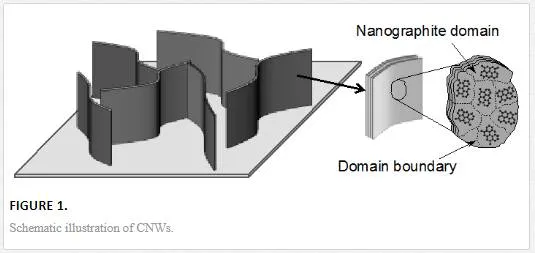
It is well known that sp2 carbon can lead to various kinds of layered structures. Among these structures, graphene (monolayer and few layers) is an actual two-dimensional material with the large anisotropy between the in-plane and out-of-plane directions. Planar graphene films with respect to the substrate have been synthesized by thermal decomposition of carbon-terminated silicon carbide and chemical vapor deposition (CVD) on metals such as nickel (Ni) and copper (Cu) substrates [1-3]. On the other hand, plasma-enhanced CVD (PECVD) is among the early methods to synthesize vertically standing carbon sheet structures [4-17]. These structures are called as carbon nanowalls (CNWs), carbon nanoflakes, and carbon nanosheets. CNWs and related nanocarbon structures consist of nanographene sheets standing vertically on a substrate. Figure 1 shows a schematic illustration of CNWs, where few-layer graphenes composed of nanographite domains form a self-supported network of wall structures. The mazelike architecture of CNWs with large-surface-area graphene planes and a high density of graphene edges would be useful as platform for electrochemical applications as well as tissue engineering such as scaffold for cell culturing [18-25].
CNWs and related sheet nanostructures have been synthesized using several PECVD techniques, which are similar to those utilized for growing carbon nanotubes (CNTs) and diamond thin films. For the growth of CNWs, typically, a mixture of methane (CH4) and hydrogen (H2) is employed as source gases. A certain amount of hydrogen (H) atoms are required for growing CNWs. In general, microwave plasma and inductively coupled plasma (ICP) have been used for the growth of CNWs. These are high-density plasmas and are suitable for decomposing H2 molecules efficiently. Or more specifically, radio frequency (rf) capacitively coupled plasma (CCP) with H radical injection and very high frequency (VHF) plasma with H radical injection have been applied to synthesize of CNWs. Pressures are ranging from 1 Pa to atmospheric pressure. Preparation of metal catalysts such as iron (Fe) and cobalt (Co) on the substrate is essential for the growth of CNTs. Unlike the CNT growth, CNWs do not require such catalysts for their nucleation. CNW growth has been conducted on several substrates including Si, SiO2, and Al2O3 without the use of catalysts at substrate temperatures of 500-700°C [5]. In view of the practical use of CNWs for device applications such as biosensors or electrochemical sensors in micrototal analysis system, further investigations should be performed to enable control of structures and surface properties of CNWs.
In this chapter, fabrication techniques of CNWs and possible applications using CNWs as nanoplatform in the area of electrochemistry and tissue engineering are described. In the beginning, characterizations of CNWs are outlined. Then synthesis method for CNWs using VHF CCP with H radical injection is presented. Radical injection technique was successfully applied to fabricate straight and large-size monolithic carbon nanosheet. The VHF CCP with H radical injection was developed with the aim of achieving large-area growth of CNWs with a reasonable growth rate. The structure of CNWs was controlled by changing the total pressure and VHF power. In addition, the structure of CNWs was modified by O2 plasma etching and hydrogen peroxide (H2O2) treatment. In the latter half of this chapter, the electrochemical application of CNWs is described. Biosensing with CNWs is a promising application. Dopamine, ascorbic acid, and uric acid are compounds of great biomedical interest, which all are essential biomolecules in our body fluids. CNWs were used as electrode to detect these biomolecules. In addition, CNWs were oxidized by the surface treatment using atmospheric pressure plasma, and proteins such as bovine serum albumin were immobilized on these surface. Electrochemical properties of surface-decorated electrodes were investigated. Moreover, CNWs were used as scaffold for cell culturing. The dependence of the cell-culturing rates and morphological changes of HeLa cells on CNW scaffolds with different densities and wettability were systematically investigated.
Brief description of carbon nanowalls
CNWs are mazelike architecture consisting of few-layer graphenes standing vertically on a substrate, as was illustrated in Figure 1. The CNW sheet itself is composed of nanodomains of a few tens of nanometers in size. Scanning electron microscopy (SEM) images of CNWs with different morphology are shown in Figures 2(a) -2(d). The morphology of CNWs depends on the synthesis conditions, including pressure, substrate temperature, source gas mixtures, and the type of plasma used for the synthesis. Typical mazelike architecture (Figure 2(a)), isolated vertical nanosheets (Figure 2(b)), and highly branched type (Figure 2(c)) have been fabricated. Moreover, straight and aligned CNWs with regular spacing (Figure 2(d)) was obtained on the substrate set perpendicular to the electrode plate in the case of growth using rf CCP with H radical injection [9]. Figures 3(a) and 3(b) show typical transmission electron microscopy (TEM) images of CNW with a micrometer-high planar nanosheet structure, which was synthesized using electron beam excited plasma-enhanced CVD [12]. Despite the relatively smooth surface, each sheet in CNWs is actually composed of nanographite domains of a few tens of nanometers distinguished by domain boundaries as shown in Figure 3(a). Graphene layers are clearly observed in the high-resolution TEM image of the CNW shown in Figure 3(b). The spacing between neighboring graphene layers was approximately 0.34 nm.
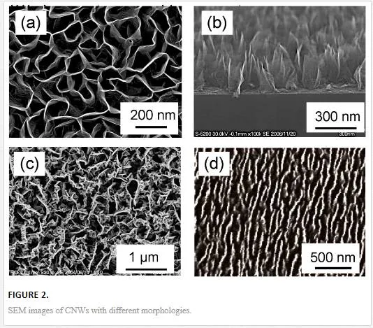
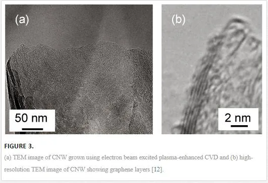
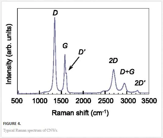
Figure 4 shows a typical Raman spectrum of CNW film formed on Si substrate, which was measured at room temperature using a 514.5-nm line of an argon laser. Typical Raman spectrum for the CNWs has two strong peaks at 1590 cm-1 (G band), indicating the formation of graphitized structure and at 1350 cm-1 (D band) corresponding to the disorder-induced phonon mode. The peak intensity of D band is comparable or twice as high as that of G band. The sharp and strong D band peak suggests a more nanocrystalline structure, and the presence of graphene edges and small graphite domains. It is noted that the G band peak is accompanied by a shoulder peak at 1620 cm-1. This shoulder peak is often designated as D’ band and associated with finite-size graphite crystals and graphene edges [26,27]. The strong and sharp D band peak and D’ band peak are prevalent features of CNWs [8,11,13]. The 2D band peak at 2690 cm-1 is used to confirm the presence of few-layer graphene. It originates from a double resonance process that links phonons to the electronic band structure [28,29].
Carbon materials such as grassy carbon and conductive doped diamond have been widely used in both analytical and industrial electrochemistry due to their low cost, wide potential window, relatively inert electrochemistry, and electrocatalytic activity for a variety of redox reactions. For the electrochemical applications, these carbon-based electrodes are often decorated with catalyst nanoparticles such as platinum (Pt). As was illustrated in Figure 1, CNW film has many graphene edges, and the CNW sheet itself is composed of nanographite domains of a few tens of nanometers in size. These graphene edges and domain boundaries are chemically reactive and are modified easily with several types of surface termination, e.g., C-NH2, C-OH, and C-COOH. Furthermore, Pt nanoparticles were preferably deposited on the defects such as grain boundaries on the surface of graphite [24]. Therefore, the structure of CNWs can be suitable for the platform of the electrochemical and biosensing applications. This kind of vertical-nanographene-based electrochemical platform with the high surface area and electrocatalytic activity offers great promise for creating revolutionary nanostructured electrodes for electrochemical sensing and biosensing, fuel cells and energy-conversion applications.
The morphology and electrical properties of CNW film depend on the synthesis conditions, including source gases, pressure, process temperature, and the type of plasma used for the growth of CNWs. We can expect a wide variety of applications based on their structure or electrical properties. For the electron emitters, CNWs with atomically thin edges, moderate spacing, and excellent height uniformity are required. For the membrane filter using honeycomb structure of CNWs, the spacing between adjacent nanowalls should be controlled. Moreover, CNWs should be detached from the substrate to obtain freestanding membrane, and the CNW membrane should be attached to the different materials. On the other hand, less aligned, dense CNW film with large surface area can be used as gas storage application, while vertical alignment and crystallinity of CNWs can be less crucial.
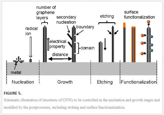
In view of the practical applications using CNWs, desirable structures and electrical and chemical properties of CNWs depend on the area of their applications. Therefore, structures, electrical properties, surface chemical properties of CNWs and related sheet nanostructures should be controlled according to their applications. Although the nucleation mechanism of CNWs is still unclear, ion bombardment on the substrate would have some effect on the nucleation of nanographene at the very early growth stage [30]. The growth of CNWs was enhanced occasionally by using metal substrates such as Ni and iron (Fe) [4]. The spacing between adjacent nanowalls and thickness of nanowalls would be affected by the density ratio of CxHy radicals to H atoms [31]. The addition of Ar into the source gas would induce the secondary nucleation at the wall surface, resulting in the formation of highly branched CNWs with high surface to volume ratio as shown in Figure 2(c). On one hand, branching could be suppressed and straight and large-size monolithic carbon nanosheet could be obtained by the addition of oxygen into the source gas [32]. In view of the practical use of CNWs for device applications such as biosensors or electrochemical sensors in the form of micrototal analysis system, postprocesses such as integration techniques, including etching and coating of CNWs and surface functionalization should be established. Figure 5 shows schematic illustration of CNW structures that should be controlled in the nucleation and growth stages and modified by the postprocesses, including etching and surface functionalization. Hereafter, we describe the recent development of CNW fabrication with emphasis on the structure control for realizing carbon nanoplatform working in the area of electrochemical and bio applications.
Fabrication of carbon nanowalls using Radical Injection Plasma Enhance Chemical Vapor Deposition (RI-PECVD)
GROWTH OF CARBON NANOWALLS FROM FLUOROCARBON/HYDROGEN MIXTURE
In the case of PECVD with hydrocarbon/hydrogen system, for example, both CH3 radical and H atoms are thought to play important roles in the formation of several carbon structures. The parallel-plate CCP might be useful to produce plenty of hydrocarbon radicals such as CH3 radicals effectively [33] and also useful for the large-area deposition of the film. However, the CCP itself is not suitable for the growth of diamond and nanodiamond films because of the shortage of H atoms [34]. In contrast, high-density plasmas such as microwave plasma and ICP are suitable for dissociating H2 molecules efficiently. Although we have managed to control radical densities in the plasma by changing the mixing ratio of source gases, it is not easy to produce multiple species with different roles effectively at the same time using single plasma. As a solution, hydrocarbon or fluorocarbon gases were excited by a parallel-plate CCP, while the H atom density around the growing surface was actively increased by the injection from the external high-density H2 plasma. This is the idea of radical injection. We have previously developed a radical-injection plasma-enhanced chemical vapor deposition (RI-PECVD) system that has allowed superior control of the properties of CNWs [5,9,10,14,15,32,35,36]. Figure 6 shows a schematic of the RI-PECVD system using very high frequency (VHF: 100MHz) plasma mainly, which was developed with the aim of achieving large-area growth of CNWs with a reasonable growth rate [10,11,14,15,32,35]. The RI-PECVD system used here is composed of a parallel plate VHF CCP and a surface wave-excited microwave (2.45 GHz) H2 plasma (H2 SWP) in tandem structure, as shown in Figure 6 [14,35]. In the case of CNW growth using fluorocarbon source gas, C2F6 was introduced into the VHF CCP region with a flow rate of 50 sccm. H2 with a flow rate of 100 sccm was introduced into the microwave SWP region, and H radicals were injected into the VHF CCP. The total gas pressure ranged from 0.6 to 1.2 torr (80 to 160 Pa). During the CNW growth, the substrate was heated at 600°C. By using this system, the heated substrate was showered with both fluorocarbon (or hydrocarbon) radicals and plenty of H atoms in a controlled manner.
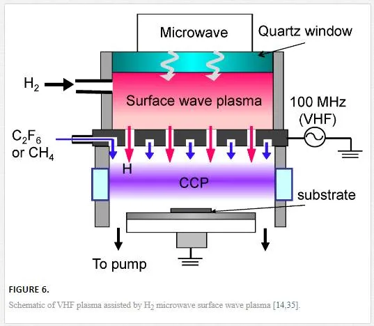
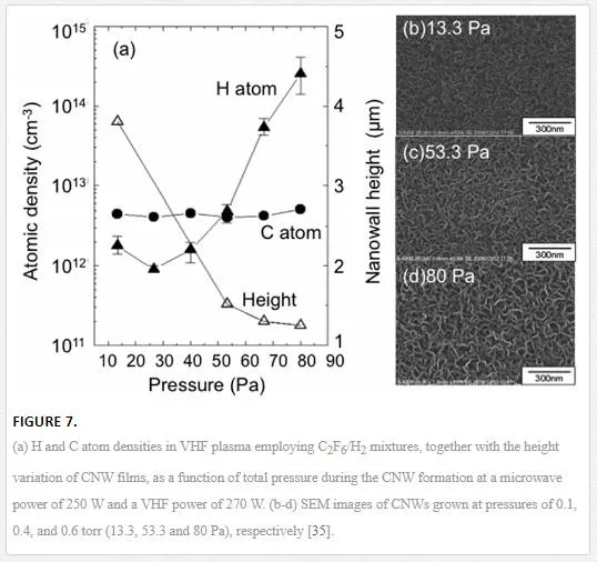
Figure 7(a) shows the H and C atom densities in the VHF plasma of RI-PECVD employing C2F6/H2mixture, together with the height variation of CNW films. The measurement of atom densities was conducted using the vacuum ultraviolet absorption spectroscopy (VUVAS) system as a function of the total pressure during the CNW growth at microwave and VHF powers of 250 and 270 W, and C2F6 and H2 flow rates of 50 and 100 sccm, respectively [35]. As the total pressure increased in the range from 0.1 to 0.6 torr (13.3 to 80 Pa), the H atom density increased drastically from 1012 to 1014 cm−3, while the C atom density was almost constant at 5 × 1012 cm−3, as shown in Figure 7(a). In contrast, the height of the CNW films decreased with an increase in the total pressure. SEM images of CNWs grown at different total pressures are shown in Figures 7(b) -7(d) [35]. CNW film with narrow interspaces was obtained at a low total pressure of 0.1 torr (13.3 Pa), while CNW film with wider interspaces of 30-40 nm was grown at a high pressure of 0.6 torr (80 Pa). As the H/C atom density ratio increased, the growth rate of the CNWs decreased and the average interspaces between the walls became wider.
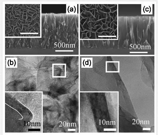
In addition, O2 and N2 gases were introduced into the VHF-CCP region. The crystallinity of vertically standing CNWs is improved by introducing O2 into the plasma used for CNW growth [32], while N addition is expected to control the electrical properties of the CNWs [35]. Figure 8(a) shows the cross-sectional SEM image of the typical CNW film grown on a Si substrate, and the inset shows the top view SEM image of the same CNW film. CNW growth was conducted on a Si substrate using a C2F6/H2mixture, resulting in the formation of slightly branching carbon sheets standing almost vertically on the substrate, as shown in Figure 8(a). The thickness of CNW film grown for 30 min was approximately 1 µm. Figure 8(b) shows TEM image of CNWs grown using C2F6/H2, where randomly oriented, small overlapping multilayered graphene domains were observed. The inset shows magnified image of the area enclosed by square, where a bent multilayered graphene structure with a thickness of approximately 9 nm was observed. In contrast, Figure 8(c) shows a cross-sectional SEM image of the CNW film grown for 40 min using C2F6/H2 with O2 addition, and the inset shows the top view SEM image of the same CNW film. CNW films grown with O2 had larger plane sheets with wider interspaces than those grown without O2. By the addition of O2 at a flow rate of 5 sccm into source gas mixture, less branching, monolithic graphene sheets were obtained, as shown in Figure 8(c). However, as a result of O2 addition, the growth rate was reduced by approximately 33%. Figure 8(d) shows TEM image of CNWs grown with additional O2, together with magnified image of square area as an inset. Monolithic self-sustaining graphene sheets larger than 200 nm in size were clearly observed in the CNWs grown with O2. A highly orientated, smooth multilayered graphene structure was clearly observed in the inset of Figure 8(d) [32].
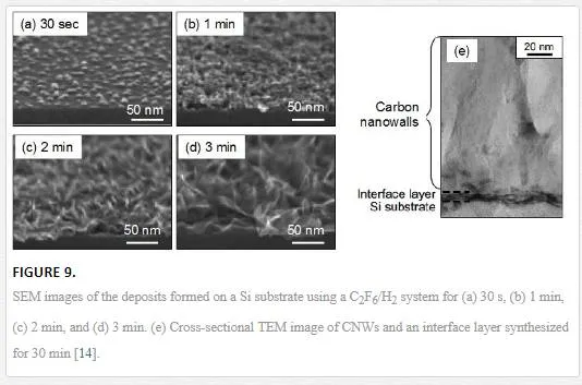
Here, the morphology and structure of deposits formed using C2F6/H2 in the early growth stage were investigated in detail. Figures 9(a)-9(d) show tilted SEM images of the deposits formed during the nucleation of CNW growth. At the very early stage of nucleation, as shown in Figure 9(a), nanoislands were formed on the Si substrate in 30 s. The density of nanoislands (number of nanoislands per area) increased with growth period. In 1 min, most of the surface of Si was covered with nanoislands (Figure 9(b)). The thickness of this layer composed of nanoislands was approximately 10 nm. At this moment, some nanoflakes have started to form at the aggregations of nanoislands forming the first layer. Subsequently, randomly oriented nanoflakes were formed on the first layer (Figure 9(c)). In 3 min, these sheet structures grow preferentially in a vertical direction to form vertical CNWs, while the number density of these nanoflakes was less than that observed at 2 min (Figure 9(d)). Figure 9(e) shows a cross-sectional TEM image of CNWs grown for 30 min, indicating that the interfacial layer exists between the CNWs and the Si surface. The thickness of the interface layer is approximately 10 nm, which is identical to the thickness of the first layer formed during the nucleation stage. Similar interface layer was also observed in the CNW films grown on Si and SiO2 substrates using inductively coupled plasma (ICP) with CH4/H2/Ar mixtures [13].
So far, several papers have been published on the observation of CNW growth in the early growth stage and the nucleation mechanism for the formation of vertical layered-graphenes on Si and SiO2 substrates using various CVD methods [5,7,8,13-17,30]. It is common in previous studies that there is an induction period of 1-5 min for the nucleation of vertical nanographene. In addition, there exists an interface layer between the vertical nanographenes and substrate surface. Raman spectra were recorded for the deposits in the initial growth stages. D- and G-bands were not observed in the Raman spectra of nanoislands formed on the substrate for 1 min or less despite the fact that carbon was detected in these samples by X-ray photoelectron spectroscopy (XPS) analysis [14]. The nanoislands and the interface layer underlying two-dimensional nanographene are considered to be amorphous carbon. In most cases using several PECVD methods, the interface layer under the CNWs is considered to be an amorphous carbon [5,7,15,17,30,37]. Due to the existence of amorphous carbon interface layer, it is possible to grow CNWs and similar structures on a variety of substrates without catalyst. In contrast, Zhu et al. suggested that graphenes parallel to the substrate surface would grow at first. In their model, at the grain boundaries of these horizontal few-layer graphenes, spreading edge of the top layers of few-layer graphenes would curl upward, resulting in the vertical orientation of these sheets [8].
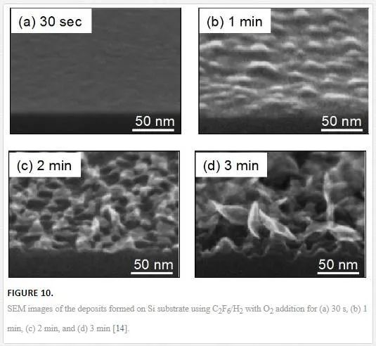
Figures 10(a)-10(d) show tilted SEM images of the deposits on the Si surface during the nucleation of CNW growth with O2 addition. At 30 s, no deposits were observed on the surface [Figure 10(a)]. In 1 min, nanoislands were formed on the Si substrate [Figure 10(b)]. It took longer time to nucleate nanoislands in the case of the growth with O2 gas addition, compared with the case without O2 shown in Figure 9(a). In 2 min, some small two-dimensional nanoflakes have started to grow at isolated nanoislands, while the fractional surface coverage was low, as shown in Figure 10(c). A distinct interface layer was not formed. As shown in Figure 10(d), isolated wall structures had grown in 3 min, while the number density of start-up CNWs was lower than that without O2,
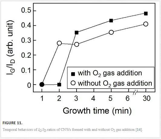
Raman spectra were recorded for the deposits formed without and with O2 addition in the initial growth stages. The intensity ratios of the G-band (IG) to the D-band (ID) of the deposits formed with and without O2 gas addition as functions of growth period are shown in Figure 11. In the case of the CNW growth without O2 addition, distinct G-band peak was observed in 2 min, and the IG/ID ratio increased gradually with increasing growth period, indicating that vertical nanographene formation started after the 2-min growth. In the case of the CNW growth with O2 addition, on the other hand, distinct G-band peak was observed at 3 min, indicating that vertical nanographene formation started after 3 min. Moreover, the IG/ID ratio was higher than that for the CNWs synthesized without O2, revealing that the O2 gas addition is effective for obtaining highly graphitized CNWs.
In the process without O2 gas addition, amorphous nanoislands were formed on the Si substrate, and the Si surface was completely covered with these nanoislands in the initial stage, resulting in the formation of a 10-nm-thick amorphous carbon interface layer. Vertical nanographene started to grow at nuclei on the surface of the interface layer. On the other hand, distinct interface layer was not formed in the process with O2 gas addition, and vertical nanographenes were formed on isolated nanoislands. O2 gas addition to C2F6/H2 is effective in suppressing the formation of carbon nanoislands and thereby in controlling CNW nucleation.
GROWTH OF CARBON NANOWALLS FROM METHANE/HYDROGEN MIXTURE
As is obvious, CNWs can also be fabricated employing the CH4/H2 mixture using RI-PECVD. In terms of controlling the wall density (or interspaces between adjacent nanowalls), total pressure and VHF power were changed. In these experiments, the heights of the CNWs were adjusted to 800 ± 50 nm, by varying the growth period. For all growth conditions, the films were uniform and exhibited a similar morphology. The thickness of individual CNWs in the films was approximately 10 nm. To consider what chemical species would affect the determination of wall density in these experiments, a plasma diagnosis was carried out using optical emission spectroscopy (OES). By introducing Ar gas into plasma region with a flow rate of 3 sccm, the actinometric measurements were carried out. Here, for determining the relative densities of H atoms and CH radicals, the emission intensity ratios ([CH]/[Ar] and [Hα]/[Ar]) were monitored by detecting the spectral lines associated with Hα 656.1 nm (excitation threshold energy, E = 12.1 eV), CH 431.2 nm (E = 14.6 eV), and Ar 751.4 nm (E = 13.27 eV).
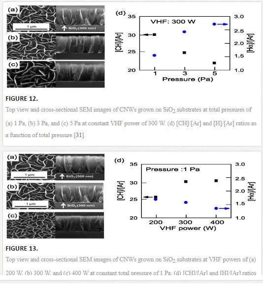
Figure 12 shows top view and cross-sectional SEM images of CNWs grown on SiO2 substrates at total pressures of (a) 1 Pa, (b) 3 Pa, and (c) 5 Pa under a constant VHF power of 300 W. As the total pressure increased, the wall density decreased or interspaces between adjacent nanowalls increased. Figure 12(d) shows the intensities of the CH and Hα emissions relative to Ar as a function of total pressure at a constant VHF power of 300 W. As the total pressure increased, [CH]/[Ar] decreased and [H]/[Ar] increased. Figure 13 shows top view and cross-sectional SEM images of CNWs grown on SiO2substrates at VHF powers of (a) 200 W, (b) 300 W, and (c) 400 W under a constant total pressure of 1 Pa. As the VHF power increased, the wall density increased or interspaces between adjacent nanowalls decreased. As shown in Figure 13(d), [CH]/[Ar] increased and [H]/[Ar] decreased with the increase of VHF power. It was found from the results shown in Figures 12 and 13 that the wall density could be controlled using the total pressure and the VHF power. The above results suggest that H and CH radicals are the important chemical species and the density ratio [CH]/[H] can be useful and simple index for controlling the wall density. Obviously, the OES provides information about only radicals of which optical emission transitions are permitted by selection rules. Other important carbon-containing species, including CH3, CH2, and C2H2 should be measured by other diagnostics such as absorption spectroscopy and mass spectrometry for further investigation on the growth mechanism.
ETCHING OF CARBON NANOWALLS
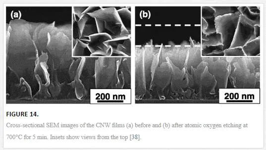
The selective oxidation techniques of the edges without modification of the graphene planes are essential for the fabrication of novel carbon nanoelectronic devices. A selective etching from the top edges of CNWs using remote oxygen plasma has been demonstrated [38]. CNW film samples were prepared on Si substrates for 30 min using the RI-PECVD system employing C2F6/H2 as described in Section 3.1. The CNW film sample was exposed to oxygen atoms provided using remote ICP source, where two electrically grounded metal meshes were installed at the exit in order to remove irradiation of electrons and ions [38]. The CNW sample was placed on the heater stage 20 cm from the exit of the remote ICP.Figures 14(a) and 14(b) show SEM images of CNW films before and after atomic oxygen etching, respectively. As a result of the atomic oxygen etching at 700°C for 5 min, the height of CNW film was reduced by approximately 160 nm, without change of wall thickness. In contrast, CNWs were not etched in the O2 atmosphere without plasma at 700°C. These results indicate that atomic oxygen would react with the top edges of CNWs preferably without ion irradiations.
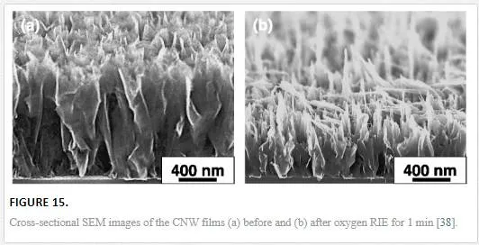
For comparison, we examined reactive ion etching (RIE) reactions using oxygen plasma. The RIE was carried out for 1 min using dual frequency (60 and 2 MHz) CCP system [38]. Figure 15 shows cross-sectional SEM images of CNW samples (a) before and (b) after oxygen RIE at 20°C for 1 min. As a result of the oxygen RIE, the height of the CNWs decreased drastically, and the top edges of the CNWs were sharpened and spearlike structures were formed.
Moreover, CNWs were subjected to hydrogen peroxide (H2O2) treatment [39]. It has been reported that H2O2 treatment can induce oxidative functional groups, such as hydroxyl groups on CNT surfaces, and can selectively oxidize disordered parts on the graphene surface [40]. Accordingly, H2O2 treatment has potential for modifying the surfaces of CNWs composed of nanographene domains. CNW film samples were prepared on Si substrates for 45 min using the RI-PECVD system employing C2F6/H2 as described in Section 3.1. The CNW film samples were treated with 30% H2O2 solution for 6 and 12 h at 90°C. Then these samples were dried in air at 110°C on a hot plate. Figures 16(a) -16(c) show cross-sectional SEM images of CNWs before and after the H2O2 treatment for 6 and 12 h. The magnified views of CNW sheets before and after the H2O2 treatment were shown in Figures 16(d) -16(f). As a result of H2O2 treatment, characteristic nanometer-scale asperities were formed on the wall surfaces of the CNWs as shown in Figures 16(d) -16(f), while the height of CNWs hardly changed. The size of the dents observed in Figures 16(e) and 16(f) was 20-30 nm. The morphology with nanometer-sized asperities on the surfaces of CNWs was stable after the H2O2 treatment. This result indicates that the radicals in H2O2 solution, such as hydroxyl radicals, react preferentially with the surfaces of CNWs at domain boundaries and induce the characteristic changes in their morphology.
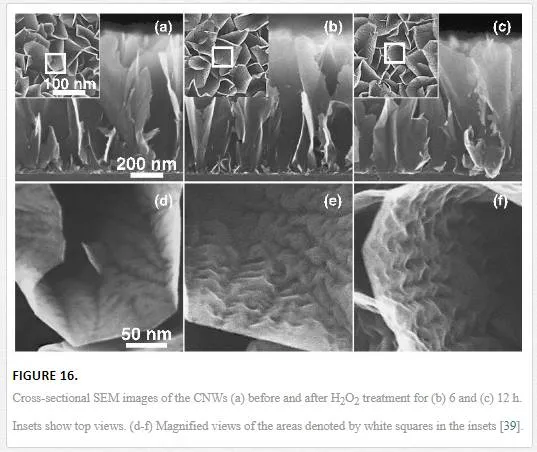
In the case of atomic oxygen etching, CNWs are selectively etched from the top edges with almost no change in wall surface morphology, as shown in Figure 14(b). On the other hand, the H2O2 treatment induces the characteristic changes in their morphology with keeping the size of CNWs constant. The nanometer-scale asperities on the CNW surface increase the surface area, which would be useful as a platform for supporting metal nanoparticles and organopollutant degradation devices [24,41]. It is noted that such asperities could be reduced by O radical exposure after H2O2 treatment, resulting in the reduction of the thickness of CNW sheets. These results, including atomic oxygen etching, oxygen RIE, and H2O2 treatment suggest the possibility of realizing etching and thickness control of walls in CNWs, which should be essential for controlling the electrical properties of graphene materials and realizing their applications to electronic devices.
Applications of nanoplatform based on vertical nanographene
PLATFORM FOR BIOSENSING
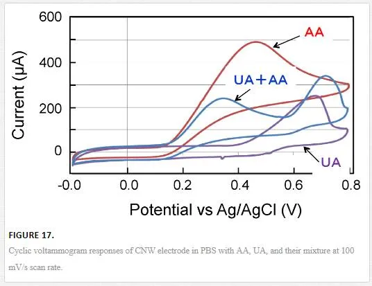
Carbon materials have been widely used in both analytical and industrial electrochemistry due to their low cost, wide potential window, relatively inert electrochemistry, and electrocatalytic activity for a variety of redox reactions. Recently, graphene has proved to be an excellent nanomaterial for applications in electrochemistry. Graphene-based materials with large surface area are useful as electrodes for electrochemical sensors and biosensors [42-44]. Electrochemical activity of CNW electrode has been investigated by cyclic voltammetry measurements in an aqueous solution of ferrocyanide and a faster electron transfer between the electrolyte and the nanosheet surface has been demonstrated [21-23]. Dopamine (DA) is a hormone and neurotransmitter that plays a very important role in the human brain and body. Since the changes in the concentration of DA are closely linked to a human’s health status, its detection has gained significant attention. Ascorbic acid (AA) and uric acid (UA) are also compounds of great biomedical interest, which all are essential biomolecules in our body fluids. Chemically reduced graphene oxide modified glassy carbon electrode was used to detect these neurotransmitters and biological molecules [42]. In these days, researches on the sensing of biological molecules became popular. Figure 17 shows examples of cyclic voltammogram responses of CNW electrode in the phosphate buffer solution (PBS) with UA, AA, and their mixture at 100 mV/s scan rate. Shang and coworkers demonstrated the excellent electrocatalytic activity of multilayer graphene nanoflakes in simultaneous determination of DA, AA, and UA in PBS [20].
Very recently, electrochemical glutamate biosensor for bioelectronic applications has been demonstrated using platinum (Pt)-functionalized graphene nanoplatelet prepared from graphene oxides [45]. Among the neurotransmitters detected by biosensors, L-glutamate is one of the most important in the mammalian central nervous system, playing a vital role in many physiological processes. The glutamate biosensor is based on the oxidation of glutamate in the presence of glutamate oxidase.

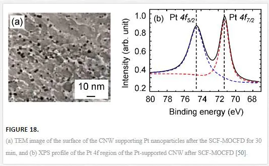
The H2O2 produced in this reaction is electroactive at electrodes such as Pt, although it is inactive at many typical carbon-based electrodes. Therefore, it is necessary to add various electrocatalytic materials such as Pt nanoparticles, hydrous iridium oxide, Prussian blue, or peroxidase enzymes on the surface of carbon-based electrodes. As was illustrated in Figure 1, CNW film has many graphene edges on the top, and the CNW sheet itself is composed of nanodomains of a few tens of nanometers in size [46]. Pt nanoparticles were preferably deposited on the defects such as grain boundaries on the surface of graphite [24]. Therefore, the structure of CNWs can be suitable for the platform of the electrochemical and biosensing applications. In many cases, Pt nanoparticles have been prepared by the reduction of Pt salt precursors such as H2PtCl6 in solution. As an alternative approach to support the metal nanoparticles on the surface of carbon nanostructures, including dense CNTs and CNWs with narrow interspaces, we developed a new method of deposition using the supercritical carbon dioxide (sc-CO2) as a solvent of metal-organic compounds. We demonstrated the preparation of dispersed Pt nanoparticles using the metal-organic chemical fluid deposition (MOCFD) employing supercritical fluid (SCF) [47-49]. TEM image of the surface of the CNW supporting Pt nanoparticles is shown in Figure 18(a). Pt nanoparticles were prepared on the CNWs by the SCF-MOCFD method for 30 min. The pressure and temperature of sc-CO2 were 10 MPa and 130°C, respectively, and the temperature of CNWs was maintained at 180°C. Pt nanoparticles were prepared preferentially at the domain boundaries of CNW surface, as shown in Figure 18(a).
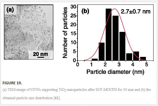
Furthermore, nanoparticles of the anatase phase of TiO2 were prepared on the entire surface of CNWs by SCF-MOCFD method at a substrate temperature of 180°C. Figure 19 shows TEM image of the CNWs supporting TiO2 nanoparticles after SCF-MOCFD for 30 min and the statistical distribution of the observed nanoparticle size [41]. For decomposing methylene blue under ultraviolet irradiation, a high photocatalytic decomposition rate of 6 mg/h was obtained for 1 mg of TiO2 supported on CNWs [41]. CNW-based electrochemical platform, which possesses large surface area with edges and electrochemical activity, offers great promise for providing a new class of nanostructured electrodes for electrochemical sensing and biosensing.
SURFACE CHEMICAL MODIFICATION OF CARBON NANOWALLS FOR THE WIDE RANGE CONTROL OF SURFACE WETTABILITY
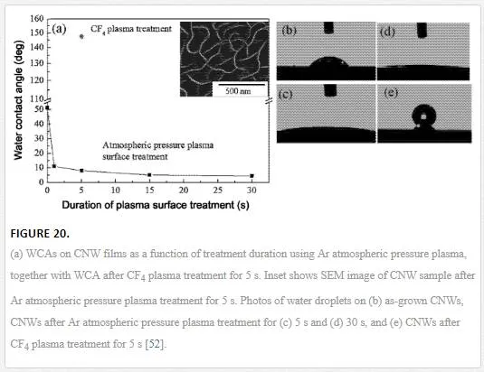
In view of the practical applications using CNWs in sensors and platforms for cell culturing, the effects of morphologies of CNWs and their surface properties should be considered systematically. We investigated the surface wettability of CNWs with emphasis on the chemisorption effect by postprocessing using plasma treatments [51,52]. Here, CNW samples grown from CH4/H2 mixtures on the Si substrate were chosen as primary forms. The surface of as-grown CNWs from CH4/H2 mixture was terminated with H atoms. After the preparation of CNW film sample using RI-PECVD for 15 min, its surface was oxidized using Ar atmospheric pressure plasma for 1 to 30 s [51,52]. The distance between the CNW film sample and the atmospheric pressure plasma source was 5 mm. We expect that soft oxidation by oxygen radicals was realized, while the effect of ion bombardment on the surface was negligible during the exposure to atmospheric pressure plasma due to the very short mean free path of ions at the atmospheric pressure. For comparison, the surface of CNW sample was fluorinated for 5 s to add hydrophobic properties to the CNWs. For the fluorination treatment, the CNW sample was exposed to CF4 plasma generated in the VHF-CCP region of RI-PECVD chamber without using H2 SWP [51,52].
After the plasma surface treatments using the Ar atmospheric pressure plasma for oxidation and the CF4plasma for fluorination in short duration, no noticeable change was observed in the morphology of CNW samples. These results indicate that such short-duration plasma treatments would induce surface chemical functionalization without etching or deposition. Figure 20(a) shows the water contact angles (WCAs) on the CNWs before and after the Ar atmospheric pressure plasma treatment, as a function of plasma treatment duration, together with the WCA after the CF4 plasma treatment for 5 s. The inset shows SEM image of CNW film sample after Ar atmospheric pressure plasma treatment for 5 s. CNW film samples examined in this experiment have all the same morphology. The side view photographic images of the water droplets on the CNWs before and after the plasma treatments are shown in Figures 20(b)-20(e). The WCAs in the case of diamond films are reported to be approximately 75˚ on the H-terminated surface and 65˚ on the O-terminated surface [26]. In contrast, the WCA on the surface of as-grown CNWs prepared employing CH4/H2 mixture was 51˚ [Figure 20(b)]. The surface of as-grown CNWs prepared with CH4/H2, of which edges and defects would be partially H-terminated, was rather hydrophilic. After the Ar atmospheric pressure plasma treatment for just 1 s, the WCA was reduced drastically to 11˚. Then the WCAs decreased gradually with further increase of the Ar atmospheric pressure plasma treatment duration. As a result of Ar atmospheric pressure plasma treatment for 30 s, the WCA on the CNWs was 5˚, indicating that the CNW surface was completely superhydrophilic [Figure 20(d)]. On the other hand, after the CNW sample was exposed to CF4 plasma for 5 s, the WCA on the CNWs increased significantly to 147˚, indicating that the surface of fluorinated CNWs was superhydrophobic [Figure 20(e)]. From these experiments, it was found that the surface wettability of CNW films could be controlled from superhydrophilic to superhydrophobic by the postplasma treatments without changing morphology.
X-ray photoelectron spectroscopy (XPS) measurements were carried out ex situ to analyze the CNW surface exposed to Ar atmospheric pressure plasma for oxidation. Figure 21 shows the composition ratio of O to C (O/C) at the surface of the CNWs as a function of plasma treatment duration. The composition ratio O/C was calculated from the peak intensity ratio of O 1s to C 1s corrected using the relative intensity factors. O content was detected even for the as-grown CNWs without plasma treatment, as shown in Figure 21. Because of ex situ XPS measurements, CNW surface was oxidized when exposed to the atmosphere. Due of the slight existence of oxygen at the surface of CNWs, the as-grown CNWs prepared from CH4/H2 would exhibit hydrophilic property as shown in Figures 20(a) and 20(b), in contrast to the hydrophobic surface of H-terminated diamond [53]. As the duration of Ar atmospheric pressure plasma treatment increased, the composition ratio O/C at the surface of CNWs increased rapidly at first, then very slowly from 5 s, and became almost constant after 15 s. C 1s photoelectron spectra after the plasma treatment were recorded (data not shown). There were various types of oxygen-related components in the CNWs after the Ar atmospheric pressure plasma surface treatment, although components related to the oxidized graphene were small. Therefore, the oxidation occurred only at the edges or surface defects, wh
ile the primary
structure of CNWs has hardly been changed by the Ar atmospheric pressure plasma exposure.
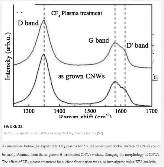
As mentioned before, by exposure to CF4 plasma for 5 s, the superhydrophobic surface of CNWs could be easily obtained from the as-grown H-terminated CNWs without changing the morphology of CNWs. The effect of CF4 plasma treatment for surface fluorination was also investigated using XPS analysis. The composition ratio of F to C at the surface of the CNWs after CF4 plasma treatment for 5 s was approximately 2.1. The composition ratio F/C was calculated from the ratio of the intensities of F 1s and C 1s peaks, corrected using the relative intensity factors. Figure 22 shows C 1s photoelectron spectrum of CNWs after the surface treatment using the CF4 plasma for 5 s. The binding energy of 284.6 eV in the XPS spectrum of CNWs is attributed to the C—C (sp2) bonds. The peaks at 289.1, 291.4, and 293.5 eV in the XPS spectrum shown in Figure 22 are assigned to the CF, CF2, and CF3functional groups, respectively [54]. These three peaks in the XPS spectrum indicate that the F-terminated surface of CNWs was obtained by the CF4 plasma surface treatment for 5 s, resulting in the realization of superhydrophobic surface.
DETECTION OF PROTEIN USING SURFACE-MODIFIED CARBON NANOWALLS AS ELECTRODES
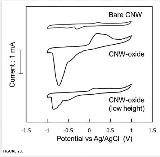
Surface-oxidized CNW films were used as electrodes to detect bovine serum albumin (BSA) in phosphate-buffered solution (PBS). BSA, a serum albumin protein derived from cows, is often used as a protein concentration standard. CNWs were grown on SiO2 substrates using RI-PECVD employing C2F6/H2 mixture [5]. For the application of CNWs as an electrode of biosensor, the surface of CNW film was exposed to the Ar atmospheric pressure plasma for obtaining superhydrophilic surface. Electrochemical measurements were conducted using a standard three-electrode setup with an Ag/AgCl reference electrode and a Pt wire counter electrode. The cyclic voltammogram (CV) profiles of as-grown (bare) CNWs (500 nm in height), oxidized CNWs (500 nm), and oxidized CNWs of low height (350 nm) were recorded at scan rate of 100 mVs-1. Figure 23 shows the CV profiles using these CNW electrodes in PBS containing BSA. In the CV profile measured using bare CNW electrode without the Ar atmospheric pressure plasma treatment, which had slightly hydrophilic surface, weak oxidation and reduction peaks were observed in anode peak potential at 0.2 V and cathodic peak potential at -0.3 V, respectively. In the CV profile using the typical oxidized CNW electrode, on the other hand, a broad oxidation and a high peak reduction currents were observed in anode peak potential of 0.2 V and cathodic peak potential at -0.75 V, respectively. The surface of as-grown CNW electrode could be easily modified into superhydrophilic one by the surface oxidation using the Ar atmospheric pressure plasma. In the case of oxidized CNW electrode with low height, the CV profile exhibited small peak currents due to the small surface area. The results in Figure 23 indicate that superhydrophilic surfaces of CNWs with large surface areas were useful as electrodes for biosensor.
CARBON NANOWALL SCAFFOLD TO CONTROL CULTURING OF CERVICAL CANCER CELLS
In recent years, cell culturing that uses carbon nanomaterials as scaffolds has been studied intensively [55-57]. The culturing rate is generally discussed with respect to the surface wettability of the scaffold. It has been reported that the cell-culturing rate would peak when the WCA on the scaffold surface is between 60˚ and 80˚ [58,59]. Moreover, many factors, including morphology, chemical termination, surface charge, scaffold surface stiffness, and the quantity of adsorbed protein are also essential for determining cell-culturing rates [60-63]. As mentioned in Section 4.2, the wide range control of surface wettability of CNWs was attained by postgrowth plasma treatments [52]. The unique features of CNWs and the variety of surface modification would give CNWs a high potential for scaffold application.
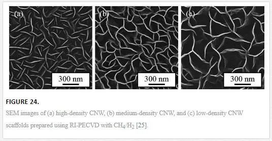
Here, the dependence of cell-culturing rate on the morphology and chemical termination of CNW scaffold was systematically investigated. Three types of CNW scaffolds with different densities (or different wall-to-wall distances) were prepared using RI-PECVD with CH4/H2 on quartz plates by changing the total pressure, CCP power, and growth period. The substrate temperature was 560°C. The flow rates of CH4 and H2 were fixed at 50 and 100 sccm, respectively. The total pressure was varied in the range of 1 to 5 Pa. The power applied to the SWP was 400 W and that to the CCP was changed in the range of 100 to 500 W. The growth period ranged from 8 to 80 min. Figures 24(a)-(c) show SEM images of the resulting CNW scaffolds with different densities. CNW scaffolds with average wall-to-wall distances of 95, 131, and 313 nm were obtained, which are denoted as “high-density [Figure 24(a)]”, “medium-density [Figure 24(b)]”, and “low-density [Figure 24(c)]” CNW scaffolds, respectively. The as-grown samples are denoted as H-terminated CNWs.
After the preparation of CNWs, some of them were subjected to various plasma treatments to realize the chemical termination of the edges and surfaces of CNWs. For oxygen termination, the CNW film was exposed to the atmospheric pressure plasma employing O2 (50 sccm)/Ar (2000 sccm) at room temperature for 30 s (O-terminated CNWs). For fluorine termination, the CNW film was set in the VHF CCP employing CF4 (36 sccm)/Ar (10 sccm) in the RI-PECVD system without SWP at room temperature for 5 s (F-terminated CNWs). The applied CCP power was 200 W, and the pressure was at 107 Pa during the plasma treatment. For nitrogen termination, the CNW film was set in the VHF-CCP region of the RI-PECVD system employing N2 (12.5 sccm)/H2 (37.5 sccm) at 560°C for 30 s (N-terminated CNWs). The applied SWP and CCP powers were 400 and 300 W, respectively. The pressure was 1 Pa. Prepared CNW scaffolds with different densities and terminations were put in multiwell cell-culturing plates. Cervical cancer cells (HeLa cells) at a density of 1.0 × 10⁴ cell/cm2 were seeded on each well. Incubation was conducted under a CO2 (5%) atmosphere at 37°C for 96 h with 2 ml/well of the medium culture. The cells were maintained in a medium of minimum essential medium (MEM) Eagle, which consisted of 5 ml of L-glutamine (200 mM), 50 ml of fetal bovine serum (FBS), 5 ml of nonessential amino acids for MEM Eagle, and 5 ml of penicillin streptomycin.
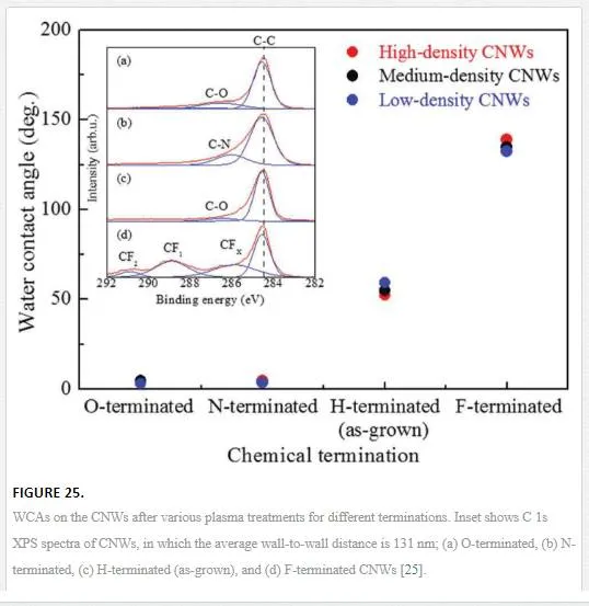
The HeLa cells cultured on the CNW scaffolds were picked up by using trypsin (0.5 w/v%, 5.3 mmol/l). After culturing for 24 h, the numbers of the cells with each of two different shapes were counted. One is the nonspreading cell with the circular shape and the other is the spreading cell with the noncircular shape [25]. Figure 25 shows the WCAs on the CNWs after various plasma treatments. The wettability of the CNWs depended on the types of chemical termination, not on the densities of the CNWs. The wettability of CNWs was controllable by plasma treatments in the range from superhydrophilic (WCA ≤ 10˚) to near superhydrophobic (WCA ≥ 150˚). The insets show the C 1s XPS profiles for the medium-density CNWs with (a) O-termination, (b) N-termination, (c) H-termination (as-grown), and (d) F-termination [52]. As shown in inset (a) of Figure 25, after the Ar/O2 atmospheric pressure plasma treatment, a small broad peak related to C-O single bonding was observed at around 286.5 eV [64]. The composition ratio O/C was 0.21. After the N2/H2 plasma treatment, a broad peak tail was observed at around 285-287 eV, corresponding to nitrogen-related bondings [inset (b)] [65]. The composition ratio N/C was 0.08. In the case of as-grown CNWs, the composition ratio O/C was 0.05. A weak broad peak related to C-O single bonding was observed at around 286.5 eV [inset (c)]. Because of ex situ XPS measurements, CNW surface was oxidized when exposed to the atmosphere. Because of the slight existence of oxygen at the surface of CNWs, the as-grown CNWs exhibited slightly hydrophilic property. In contrast, after the CF4/Ar plasma treatment, sharp peaks related to C-CFX (X ≤ 3) bonding structures were evident as shown in inset (d). The composition ratio F/C was estimated to be approximately 0.49.
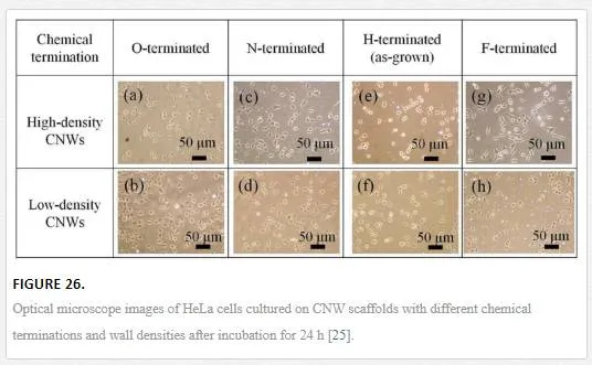
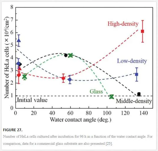
Optical microscope images of HeLa cells cultured on the CNW scaffolds with different terminations and wall densities after incubation for 24 h are shown in Figure 26 [25]. The numbers and morphologies of cultured HeLa cells somewhat depended on the chemical terminations as well as on the wall densities of CNW scaffolds. Figure 27 shows the numbers of HeLa cells cultured on the CNW scaffolds after incubation for 96 h as a function of WCA. For comparison, HeLa cells were also cultured on commercial glass plates, and the maximum number of cells was achieved at a WCA of 60˚, as previously reported [66]. Similarly, on the medium density CNW scaffolds, the maximum number of cells was obtained at a WCA of 55˚. In the case of low-density and high-density CNW scaffolds, however, the number of cells decreased and increased, respectively, with increasing WCAs. Hence, superhydrophilic surface is suitable for cell culturing on low-density CNW scaffolds, while superhydrophobic surface is suitable for high-density CNW scaffolds. As was shown in Figure 25, the surface wettability was nearly independent of the wall density. On the other hand, the cell-culturing rate was strongly dependent on the wall density of CNW scaffolds. These results suggest that the surface wettability is not dominant factor for determining the cell-culturing rate, while it is useful as approximate index of the expected cell-culturing rate. These experimental results indicate that the density of CNWs is the most essential factor for cell culturing rather than the surface wettability and types of chemical termination of CNW scaffolds. However, detailed mechanisms of cell/scaffold interactions in cell culturing on CNW scaffolds have not yet been clarified.
As a result of systematic investigation on the cell-culturing rates and morphological changes of HeLa cells on CNW scaffolds with respect to the wall densities and wettability of CNWs, it was found that the cell-culturing rates were significantly dependent on the CNW densities but seemed to be independent of the surface wettability of the CNW scaffolds. These results enable us to understand the detailed mechanisms of cell culturing on such scaffolds. Moreover, findings in the present study should also contribute to realize various nano-bioapplications using carbon nanomaterials.
Conclusion
Carbon nanowalls and related nanocarbon structures composed of nanographene sheets standing vertically on a substrate have been studied intensively. The mazelike architecture of carbon nanowalls with large-surface-area graphene planes and a high density of graphene edges and domain boundaries could prove useful for a number of different applications. Fabrication techniques of carbon nanowalls and possible applications using carbon nanowalls as nanoplatform in the area of electrochemistry and tissue engineering have been described. A radical injection technique was successfully applied to fabricate straight and large-size monolithic carbon nanosheet. The morphology of carbon nanowalls was controlled by changing the total pressure and input power. In addition, the structure of carbon nanowalls was modified by O2 plasma etching and H2O2 treatment. Using carbon nanowalls as a platform would be the most promising and important application. Carbon nanowalls were used as electrode to detect several biomolecules. In addition, carbon nanowalls were oxidized by the surface treatment using the atmospheric pressure plasma, and proteins such as bovine serum albumin were immobilized on these surface. Moreover, carbon nanowalls were used as scaffold for cell culturing. The dependence of the cell-culturing rates and morphological changes of HeLa cells on carbon nanowall scaffolds with different densities and wettability were systematically investigated.
Nanoplatform based on vertical nanographene offers great promise for providing a new class of nanostructured electrodes for electrochemical sensing, biosensing, and energy conversion applications
