The electrons “boxed up” or confined in quantum confinement and the calculation of their energy levels, which are well known from textbooks, were regarded for decades as idealistic concepts far from practical reality. The molecular beam epitaxial (MBE) technology, developed for compound semiconductors, made the introduction of the low-dimension structures into the everyday scientific research possible. The structures confined in all three dimensions are called quantum dots (QDs). For the fabrication of QDs or any zero-dimensional structures, various methods were developed. For a long time, the only known method for the production of epitaxially grown zero-dimensional system was the strain-induced method, based on lattice mismatch. Presently, the most used technique is the lattice-mismatched technique by the Stranski–Krastanov mode [1–5]. QDs, such as InAs nanocluster prepared on GaAs surface, are the oldest known system. The droplet epitaxy (DE), however, is one of the latest methods for QD preparation. This method of preparation is not only an alternative way to the conventional method but also a production method for a number of zero-dimensional quantum structures such as ringlike QDs, double ringlike QDs, inverse QDs (filled nanoholes), or QD molecules. This technique is also fully compatible with MBE technology.
The subjects of this paper are the technologies used, growth kinetics, and some properties of the zero-dimensional nanostructures of different shapes, grown by DE. The fundamentals of DE were first demonstrated by Koguchi and his coworkers in the early 1990s [6–9]. One advantage is that it is not restricted by mismatch conditions; in addition to that is the possible fabrication of strain-free QDs and similar nanostructures by DE, against the Stranski–Krastanov-based growth method. The shape diversity makes it a preferable process for that application. The size, shape, and elementary distribution of the developed structures are dependent on the developing technology used. It is obvious that the physical parameters of the structures are important from both the theoretical and practical point of view. In this paper, QDs grown by DE will be described, selected from III and V class materials. Here, the QDs are mostly GaAs with the use of AlGaAs as barrier material. This process consists of the following two basic steps: first, the metallic (e.g., Ga) nanosized droplets are generated on the surface by the Volmer–Weber growth mode, followed by the second step of droplet crystallization that is the transformation into GaAs QDs in arsenic atmosphere. For the control of the process, the kinetics of the growth process knowledge is necessary, which is so far lacking the full theoretical description.
The DE technology for QD preparation has superiority over the nowadays widely used strain-induced method. The greatest advantage is that both lattice matched and mismatched can be used for QD fabrication. At the same time, the size and density of the QD’s can be controlled independently, and the distribution is more uniform. However, the shapes of the QDs show a wide spectrum. This spectrum includes the conventionally shaped QDs, ringlike QDs, and complex multicomponent QD structures [9–13]. To avoid intermixing, low temperature can be applied at preparation. A wide variety substrate orientation has beneficial effect on the application. Although the technique is quite recent, it is already successfully applied in a number of cases. QDs had significantly improved the general performance of the optoelectronic devices, like semiconductor lasers and optical amplifiers. DE fabricated QDs introduced further improvements for the beneficial reasons described previously [10]. Future quantum devices, based on quantum mechanical and electromagnetic interactions, require lateral QD configurations. With the modified DE method, aligned QD pairs and QD molecules can be produced without involving lithographic technology [14, 15].
The droplet epitaxial technique
TECHNOLOGICAL BACKGROUND AND PRELIMINARIES OF THE DROPLET EPITAXIAL TECHNIQUE
It is well known in our profession that the grown structure can be classified in three growth modes depending on the interaction among the constituents. These modes are the layer-by-layer growth or Frank–van der Merve mode, the island growth or Volmer–Weber mode, and the intermediate mode (layer-plus-island growth) or Stranski–Krastanov mode (Figure 1) [16]. The morphology of the interface is determined by the interplay between deposition, desorption, and surface diffusion. If an atom or molecule from the environment arrives at a random position on the surface, the deposition process bonds with the surface atoms and sticks.
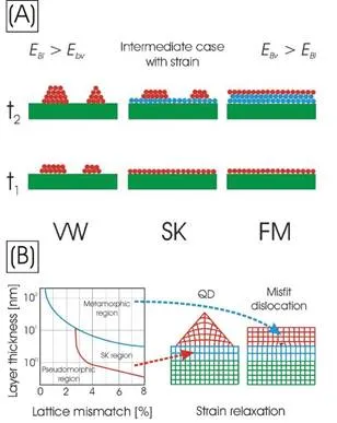
The process competing with deposition is desorption. During the desorption process, some atoms deposited on the surface leave the interface. The probability of the desorption depends on how strongly the atom is bonded to the surface. The strength of the bonds depends either on the type of atom or on the local atom arrangement of the surface where the atom sticks. The desorption can be negligible for many materials under typical MBE conditions. The deposited atoms diffuse on the crystal surface, searching for the energetically most favorable position. The diffusion length can be quite large and depends on the temperature and the binding energies to the substrate (EBv, binding in vertical direction). In the Frank–van der Merve mode, the interaction between the neighboring atoms (EBl, lateral directions) in the layer is weaker than that with the substrate atoms (EBv > EBl) [17]. In this growth mode, islands of monolayer (ML) height coalesce before a new layer can nucleate on top of them. In the Volmer–Weber mode, the situation is just the opposite, that is, the binding energy among the deposited atoms is stronger than to the substrate surface (EBl > EBv). In this case, the growth proceeds to many atomic layers at discrete islands before these islands merge. In the Stranski–Krastanov mode, the process is initiated in a layer-by-layer fashion, but islanding commences after the growth of a certain layer thickness. In certain situations, layer-by-layer growth is desirable because of the need for multilayered structures with exact layer thickness and flat interfaces. This requires that the nucleation takes place as a single event on the substrate. In this growth mode, the lattice mismatch between the grown layer and the substrate material is the most common case.The deformation takes place by the even layer to match the lattice of the substrate. In this case, elastic energy is generated in the structure, which deforms mainly the lattice of the grown layer.
When this deformation energy overcomes a critical value, it can be relaxed in two ways. One possible way is to nucleate nanosized islands on the surface of the even layer, which is called the wetting layer. The absence of the lateral layer allows the atomic planes to laterally relax, reducing the elastic energy in the structure. According the first mentioned way, the so-called strain-induced QD can be grown. The other way is to generate misfit dislocations at the interface [18–21]. The dislocations in the substrate and at the interface can overgrow into the grown layer [23–25]. These defects are called threading dislocations.Figure 1
shows the following two out of three growth modes, Volmer–Weber and Stranski–Krastanov for nanostructure production. One may ask why only the Stranski–Krastanov growth mode is widely used for QD production. The answer lies in the development of the MBE technology. The application of III–V materials opened the way for the production of heteroepitaxial structures, specifically the GaAs–AlGaAs–AlAs system, for its identical lattice parameter. The growth of InAs and InGaAs created particular technological difficulties due to the lattice mismatch. In the early 1990s, the success of InGaAs growth on GaAs, with differing indium content [26–27], brought about a big advance in this field. Initially, the thickness of the layers stayed under a critical value, but this limitation was successfully overcome. The strain-induced QD production has superseded the DE, dominating the field earlier. The archetypal system of the clustered nanostructures is the lattice-mismatched system such as InAs on GaAs, where the strain-induced process leads to the formation of QD. The lattice-mismatched structure can relax either by the generation of misfit dislocation or by the nucleation of nanosized islands on the even layer (Figure 1). The essential driving force for coherent QD formation, after an under layer formed, is the strain relaxation, whereby the energy gained from the increase in surface area via QD formation more than compensates the increase in interfacial free energy. It is generally accepted that one of the essential driving forces, for coherent lattice-mismatched QD formation, is strain relaxation. The field of self-organized strain-induced QDs is dominated by two material system, InAs/GaAs (001) and Ge/Si (001). For instance, the MBE growth of about 1.5 MLs of InAs on GaAs results in the spontaneous formation of InAs QDs driven by the strain between the deposited InAs and the GaAs substrate. The driving force for the self-organized QD formation is the strain energy induced by the lattice mismatch of about 7%, in which the condition restricts the material choice. Two families of the shape such as pyramids and domes can be created during the defect-free QD transformations [28].
PRINCIPLES OF DE
The QD preparation in a self-assembled manner by using the DE technique is an advantageous alternative and extension to the strain-induced QD creation. The basic idea of the DE originated from Koguchi and his coworkers [29, 30]. In comparison with the technology of the strain-induced Stranski–Krastanov QD production, the DE is more flexible regarding the choice of the QD material and also regarding the shape and distribution of the resulted QDs and other unconventionally-shaped QD structures. For example, it is possible to create not only InAs QD on GaAs but also strain-free GaAs QD on AlGaAs surface. Furthermore, this technology of DE allows us to produce ringlike QD and further special-shaped nanosized structures and structure complexes [31–35].
In the case of the DE, the clustering on the surface is carried out with the help of Volmer–Weber like growth mode. The basic idea based on the separation of the III-column and V-column materials supply during the MBE growth (Figure 2). Here, the QD preparation consists of two main parts such as the formation of metallic nanosized droplet on the surface and its crystallization with the help of the non-metallic component of the compound semiconductor. It is very important to mention that this DE technique is entirely compatible with the MBE technology. This circumstance allows us to combine the DE method with the other conventional MBE processes.
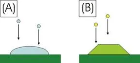
First, the III-column elements such as Ga, In, Al, etc., are deposited. These metallic components form clusters that are nanosized droplets on the substrate surface. At the droplet formation, the main driving forces are the diffusion, the minimalization of the surface tension, and the Ostwald ripening [36–42]. The dominance of these driving forces depends on the technological circumstances. The second step of the DE technique is the crystallization of the metallic cluster by the molecular beam irradiation of the nonmetallic V-column element. It is important to suppress or to control the lateral diffusion of the group III elements from the cluster.
QD ENGINEERING
As known, the electronic and optoelectronic properties of the nanostructure depend strongly on the shape of the nanostructure. The technology used for growth can be controlled by the size, shape, and elementary distribution of the developing structure. These technological and physical parameters are very important from both theoretical and practical points of view. In the DE technique, because of the shape and distribution diversity, the key point is to discover growth mechanism and its relation with the parameters of the developed structures. Since the discovery of the DE, several scientific knowledge are gathered. However, until now, no full theoretical description of the underlying growth kinetic is available.An interesting correlation between the GaAs QD shapes and their volume was observed by Heyn and coworkers [43, 44]. As a result of this discovery, they developed the first growth model for the DE of GaAs QDs [43, 44]. The experiment was carried out with the cystallization of Ga droplets on AlGaAs surface. Here, growth temperature ranged between 140°C and 300°C. On the arsenic terminated surface, the deposition of Ga with flux 0.025–0.79 ML/s was executed. It was clearly visible that growth temperature strongly influenced QD density.
The QD density dependence on temperature shows the scaling law [44]. Under 200°C, the slope of the temperature shows Ea = 0.235 eV. Over 200°C, data did not follow the scaling law, but QD density decreased. At this temperature, coarsening of the cluster begins. This effect goes back to the Ostwald ripening, which means the growth of large clusters at the expense of smaller ones, hence causing a decrease in the total cluster density. Higher temperature combined with lover arsenic flux will result in a ringlike nanostructure. At longer waiting time and lower arsenic flux, these rings fall below the original substrate surface and the encircling surround. After the heat treatment of the sample with the clusters formed, the total lack of arsenic results in nanoholes. The creation of nanoholes can lead back to the thermal etching of the substrate by the liquid metallic component. At a typical process temperature of 570°C, etching starts approximately 20 s later than the beginning of the annealing step, followed by desorption approximately 100 s after. The depth of the nanoholes can be found by multiplying the etching time by the etching rate. These nanoholes can be filled with low band-gap material to create the so-called inverted QD. Furthermore, the nanoholes can serve as templates for QD preparation. In the utilization of surface anisotropy, QD pairs can be grown. The nanohole and the nanomound can initialize QD molecules, where the QD per molecules ranged from two to six. In the case of InAs QDs on GaAs (001) surface, the number of QDs per GaAs mound can be effectively controlled by varying InAs ML coverage [45].
Droplet formation
THE INITIAL SURFACE STATUS
During the QD formation, the status of the substrate surface is very important. It is well known that surface reconstruction influences strongly the growing layer and the forming structure [16]. Surface reconstruction depends on the temperature and the ambient environment environment, too. As mentioned before, the DE technique is compatible with the MBE technology. It means that the growing surface can be continuously monitored with reflection high-energy electron diffraction (RHEED) to determine the status of the surface, e.g., the surface reconstruction. During the growth, the RHEED pattern and its specular spot intensity allows a real-time tracking of the surface status changes. Here, we are using the technological most important (001) surface orientation. The bipolar (001) surface of GaAs can be terminated by either Ga or As atoms with rich variety of reconstructions are formed depending on surface stoichiometries [16].Before the droplet creation, we have to grow a layer from a wide band-gap material for barrier. This layer growth happened with a conventional MBE technology, which is carried out in arsenic ambient pressure. Hence, the initial status of the surface is arsenic terminated. After the layer growth, we have to change the temperature depending on the planned nanostructure shape. The deposited MLs are not equal with the droplet volume. Assume that Ga is deposited on AlGaAs surface at 200°C. Due to the strong binding energy of As to Ga and substrate, the first Ga ML is consumed for the formation of Ga terminated surface. This first ML volume does not contribute to the formation of the Ga droplets. It means the coverage of Ga located in the droplet is Ft–A. The total Ga surface coverage is Θ = Ft, where it is resulted with flux F for a time t, and A is the incorporated value of ML.
Although no complete phase diagram of GaAs (001) has been mapped, certain surface phases are generally observed during growth or after growth and annealing. For example, the less As-rich surface exhibits a (2 × 4) / c(2 × 8) pattern and arises from 0.75 ML of As. This reconstruction is normally present during the MBE of GaAs. Areas with (2 × 4) and c(2 × 8) symmetry can coexist. With larger coverage of As, a c(4 × 4) reconstruction with As coverage of 1.75 ML is observed [46, 47]. Depending on the substrate temperature and the Ga-to-As ratio during MBE, the GaAs (001) surface is known to display various surface reconstructions ranging from the As-rich c(4 × 4)β, c(4 × 4)α, c(2 × 8), and (2 × 4) to the Ga-rich (6 × 6), c(8 × 2), (4 × 6), and (4 × 2) surface. The surface symmetry critically depends on the preparation conditions [46, 47]. In situ investigations of this large set of reconstructions with RHEED are well established. Using scanning tunneling microscopy (STM), most of these surface reconstructions could also be imaged in real space, and the structure and the structural models were refined, too. Most of the previous studies were based on the diffraction techniques and no direct observation for the (4 × 6) phase exists. The STM study reveals that (4 × 6) symmetry arises from the coexistence of (2 × 4) and (4 × 2) units [48]. We have seen before that the change in temperature and other parameters results in the continuous change in surface reconstruction. During the change of the temperature, not only the reconstruction but also the specular spot intensity changes. The results show that at lower temperature, the specular spot intensity is high, and at higher temperature, the intensity is low. Furthermore, in the up and down and back directions, the temperature versus intensity function shows hysteretic behavior (Figure 3). The explanation of this phenomenon can lead us to the understanding of the intricate surface structures [49, 50].
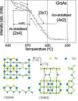
The initial step of the DE is the droplets creation on the surface. It is already well documented that the droplet nucleation requires Ga-terminated surface, which means that a part of Ga coverage incorporate into the surface. During the initial stage of Ga deposition, fundamental change happens in the surface reconstruction, which strongly influences the droplet formation. Before the Ga deposition, the surface reconstruction can be usually c(4 × 4), (2 × 4), or (4 × 6), where the values of As coverage are 1.75, 0.75, or 1.12 ML, respectively. The previous paragraphs show the complicity of the surface reconstruction and other difficult unsolved problems associated with the process. The part from the metallic surface deposition migrating into the droplet depends largely on the initial state of the surface.
SIZE AND DENSITY OF THE DROPLETS
The size and the density of the metallic droplets depend on the substrate temperature and on the deposited MLs. In the case of Ga droplets on AlGaAs surface under 200°C, the cluster density versus temperature follows scaling law. Over 200°C, the scaling law is broken. Under this temperature, the clusters begin to coalesce, which drastically reduce the cluster number. This decrease of cluster number is governed by the Ostwald ripening [36–42]. The reduction of the cluster number is affected by the diffusion length of the constituents. The condition required for the coalescence is the overlap of the diffusion length and the mean distance of the neighboring clusters. It characterized by a local interaction between neighboring clusters of slightly different size. The smaller cluster starts to decompose to maintain the gradient of the radius equilibrium concentration toward the larger cluster due to the Gibbs–Thomson effect [51]. The appearance of such processes is critically dependent on the initial conditions. The Ostwald ripening describes the driving force, which determines the size distribution of cluster ensemble on the surface [38–40, 42, 52]. This description supposes a driving force that depends on the mean radius of the islands. It is supposed that atoms detach more readily from smaller islands and condense rather to larger ones. Therefore, for a given amount of material on the surface, larger islands grow at the expense of smaller ones. The temporal evolution of the island radius (r) can be described by a differential equation: dr/dt = b(T) / r2(1/r – 1/rc), where rc is the critical cluster radius and b(T) is a temperature-dependent parameter.
DROPLET–SURFACE INTERACTION
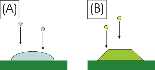
In this section, we will discuss the interaction between the droplet and the substrate surface. Here, the dependence of the droplet shape and the so-called thermal etching are discussed. It is known that the droplet shape is determined by the wettability of the substrate surface, and this property can be described by contact angle. There are three types of situations: no wetting, partial wetting, and complete wetting, where these situations correspond somewhat with the three growth modes. The contact angle depends on some circumstances, such as the status of the carrier surface, the droplet size, and the temperature. This is because the nuclei may wet the substrate, strongly changing their geometry. The deposited material will not wet the substrate because this would be accompanied by an overall increase in free energy of the system. The liquid deposit will spread out to maximize the area of the interface. For all the other situations, a partial wetting with a contact angle θ should be considered, that is, γs = γi+ γecosθ, where γe and γs represent the surface free energies of deposited cluster and substrate, respectively, and γi is the interfacial free energy (Figure 4) [53].
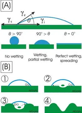
In our DE case, we have to discuss a further interaction between the droplet and the carrier surface. This interaction is called thermal etching, droplet etching, or local droplet etching. The explanation of the process will be discussed with the help of Ga/GaAs/AlGaAs system. Where Ga droplet forms on AlGaAs surface.It is known from the liquid phase epitaxy that thermal etching takes place at the interface Ga melt and AlGaAs surface [54–57]. In the first step in DE technology, Ga droplets are generated on the surface. Due to thermal etching, this droplet-shaped Ga melt can solve the arsenide from the substrate material. At the interface, the metallic components of the substrate mix with the Ga atoms of the droplet. During the QD formation, this thermal etching takes place, too. In the initial stage of the QD formation, enough time is available for the mixing of the atoms at the interface. In the case of GaAs QD on AlGaAs substrate, Al content can be observed in the GaAs QD. This phenomenon was confirmed by the author and coworkers [58]. This thermal etching effect can be observed also at evolution of the ringlike QDs.
Our observations show that the middle part of ringlike QDs is below the surface of the substrate surrounding the QDs. This phenomenon is also the consequence of thermal etching. At slow crystallization, etching can act longer; therefore, it results in deeper holes in the center. At high temperature, quite deep nanohole can be achieved [85].Thermal etching can be utilized also for nanostructure preparation. With the help of droplets created on the substrate surface, the surface can locally be etched. At higher temperature, this etching phenomenon is more significant. After the local thermal etching, the remained deep craters are the so-called nanoholes. During the DE QD fabrication, the Ga deposition temperature is ranged between 100°C and 350°C typically. These temperatures are very low compared to usual MBE growth conditions. In this case, the droplet thermal etching is less significant. At significant higher temperature, the situation is different.
If the temperature ranged between 450°C and 620°C, the local thermal etching under the droplet is already considerable. After an annealing time, the droplet is replaced in a nanohole surrounded with lobes. This local droplet etching shows a very promising technique for the structuring of the substrate surface without any lithographic processes. Furthermore, this patterning is also fully compatible with the MBE technology. In this way, nanohole was first presented by Wang and coworkers [59].This finding opened a new way for the fabrication of another type of QD. This system was based on the filling of the nanohole, where the fill of the hole is carried out with lower band-gap material than the substrate. In this way created, nanohole filled inverted QDs are demonstrated by Heyn and coworkers [60–66]. In the process of nanohole filling, we utilize the Ga diffusion on the substrate surface. The temperature and orientation dependence of the Ga (and other metallic component) diffusion can be utilized at further nanostructure preparation.
Formation of QD
PREPARATION TECHNOLOGY
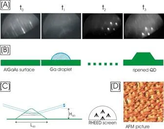
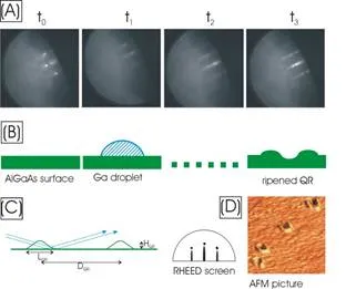
The initialization of the alternatively grown conventionally shaped QD preparation, the basic idea of DE, originated from Koguchi and his coworkers [6, 30]. In this way, it is possible to create strain-free GaAs QD on AlGaAs surface. Along this discovery, further unconventionally shaped QD types were discovered [9, 32–35]. In the following, we will detail the DE-grown single hump-shaped QD in the case of GaAs/AlGaAs system. As discussed above, this process consists roughly of two main steps. First, metal (in our case Ga) droplets are generated on the surface in a Volmer–Weber-like growth mode. In the second step, crystallization takes place. Under arsenic pressure, the droplets transform into crystalline nanostructures. The shape of the nanostructures and their distribution depend on the initial droplet size and distribution and on the further technological parameters such as substrate temperature, arsenic pressure, waiting time, etc.Here, typical experimental parameters for conventional QD preparation are described [43]. The GaAs QDs are grown on AlGaAs (001) surface. The growth experiments are performed in a solid source MBE system equipped with effusion cells for Ga and Al evaporation and valved cracker cell for arsenic ambient pressure. The evolution of growth front is in situ monitored with RHEED. First, on GaAs (001) wafer, pure GaAs layer is grown, and it is followed by an AlGaAs layer with Al content of 0.3. After the AlGaAs layer preparation, the sample is cooled down to 200°C. The θ = 3.75 ML Ga is deposited with the flux of 0.75 ML/s without any As flux. After the Ga deposition, a 60-s waiting time is performed. The annealing is carried out at a temperature of 350°C and at an As pressure of 5 × 10⁻⁵Torr. The growth process are tracked continuously in the direction of [11¯1¯0] with the help of RHEED [67]. In this direction, the RHEED pattern is more informative for the status of the QD evolution compared with the perpendicular [110] direction. After the growth process, the quantum objects can be ex situ investigated (AFM and TEM and PL methods), which can provide us further information to understand the growth kinetics.During the QD preparation, the sequence of the RHEED pictures in the main growth stages is depicted in Figure 5. In the initial stage, the RHEED pattern showed sharp streaks (stage at t0). After the Ga deposition, the pattern diffused on the RHEED screen (stage at t1). Almost at the same time with the offering of arsenic pressure, the RHEED pattern changed suddenly from diffused to spotty (stage at t2). During the annealing phase, the pattern changed slowly (some minutes) from spotty to spots with tails (stage at t3). The density of QDs is 3.6 × 1010 cm–2. It is shown that the characteristic RHEED pattern of QD is still recognizable even if the dot density is one order of magnitude less [43].
GEOMETRY AND ELECTRONIC STRUCTURE OF QD
As we demonstrated earlier, the shape of the QDs depends on the volume and also the density of QDs. According the shape, there are two types of QDs. The larger type of QD is a truncated pyramid-like shape with side facets of 55°. The smaller QD is a pyramid-like form with a side facet of 25° [43, 44]. In the following, the geometry of the QD will be discussed in the case of the smaller type of QD.The atomic resolution structure of a typical DE-grown QD is shown in Figure 6. (The image was taken with the electron beam parallel to the [110] zone axis of the AlGaAs single crystal substrate [43, 67–68].) The typical dimensions of the QD shown in Figure 6 are 54 nm base width and 5.5 nm height. The steepness of the QD side wall measured by TEM as well as by AFM shows about 25°. Figure 6 also shows that all the lattice fringes of the AlGaAs substrate are continued in the GaAs QD without any distortion. It is well known that the lattice parameters of these two substances are practically the same. No crystal defects were observed within the QD or at the interface with the host crystal [68, 69].
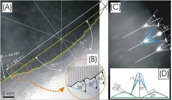
The feature mentioned is shown in a darker contrast of the QD, also a few atomic surface layer of AlGaAs crystal between the QDs. The darker contrast on the AlGaAs surface can be interpreted as follows. The AlGaAs layer, at low temperature, shows As-rich c(4×4) surface. Nominally, θ = 3.75 ML Ga is deposited on the surface without arsenic flux. In the duration the Ga supply, a few ML of Ga is combined with excess arsenic surface atoms. Thus, a thin GaAs layer forms on the surface while the rest of the Ga forms nanodroplets. During the crystallization, the droplet and the surface layer go into similar composition. As a result, the QD and the surface layer shows similar darker contrast compared to the host material [69]. The existence of this GaAs surface layer was predicted earlier from the comparison of the PL measurement and the energy level calculation [32].The chevron tails are connected with the faceting of QDs as it was verified in the case of diverse-shaped DE QDs [10]. In case of DE, it can be shown from the AFM measurement and from the tilted TEM picture that the shape and size of QDs are very uniform [69], and their side angle is about 25° [43, 68], which corresponds to the half opening angle of the chevron tails (Figure 6). Despite the same shape of the QDs, the chevron tails are not sharp but broad [68]. The observed side angle near to 25° corresponds to the (113) crystallographic plane [67, 68].
A cross-sectional TEM image shows that the side of the QD is not a single crystalline plane but has stepped shape (faceting). The steps consist of planes parallel with interface (parallel with {002} crystal planes) and planes with 55° to the interface, corresponding to {111} planes. The envelope curve of the QD cross section is a circle segment with a radius of R = 64 nm [68]. The electronic structure of the DE-grown GaAs QDs was investigated by PL spectroscopy [70, 71]. Furthermore, lasing was demonstrated in such structure [72]. After postgrown annealing, improved optical performance was demonstrated [72]. In the case of DE-grown QDs, the better optical properties compared to strain-induced QDs originated from the technology. The DE-grown QDs are prepared at very low substrate temperatures, which are unfavorable in view of the incorporation of undesired background impurities and crystal defects.
SOME ASPECTS TO THE KINETICS OF QD GROWTH
The growth kinetic can primarily be investigated by the in situ RHEED tracking. In the annealing phase of QD production, the diffused RHEED pattern becomes spotty nearly simultaneously with the opening of arsenic source. The sufficient arsenic quantity and the low temperature make the build in (infiltration) of As in the Ga phase (i.e., crystallization) possible [73]. This process of infiltration takes about 2–3 min to the sharp chevron image. A crystallized shell comes into being on the Ga droplets. The spotty RHEED pattern originates from the transmission electron diffraction. The electron beam goes through the crystalline GaAs shell layers over the droplet. If there are crystallite formation or droplets on the surface, It is observed that bulk scattering of the grazing beam can occur and the RHEED pattern may become dominated by spots rather than streaks due to transmission electron diffraction (Figure 5) [67].
The scattering from several planes strongly modulates the intensity along the reciprocal lattice rod. Thus, the streaks observed from two-dimensional surface are not observed when transmission dominates [67]. For the transmission case, the reciprocal lattice is an array of points each broadened owing to the finite size of the scattering region. During the annealing, the As diffuses inside of droplets, while excess As builds in (infiltrates) in the shell [73, 74]. Thus, the droplet crystallizes slowly. In the given moment, the rounded shell will be broken by the cornered crystallite grown inside of the structure. At the same time, a chevron-shaped spot develops on the RHEED screen [43, 48, 67, 68]. The angle between two RHEED streaks starting from same reciprocal lattice point is about 55°, as shown in final stage of the QD evolution. These so-called chevron tails are attributed perpendicularly to the facets of the QD [67, 69]. The volume of the QDs is large enough to receive transmission pattern during the electron scattering. The main lateral expansion LQD and height HQD of QD – according to the AFM measurement – are 50 and 5 nm, respectively (see Figure 6). The mean free path of the electrons Λ in GaAs between the crystal planes without collision at the typical incidence angle of RHEED (about 2°) is less than 20 nm. Thus, in our case, there are several (ca. 9) lattice planes to receive transmission character [67].
The analytical TEM investigation provides further contribution to the evolution kinetics. In our TEM investigations, we detected Al content in GaAs QD [48]. Here, this study shows the high-resolution micrograph of a similar QD together with Ga and Al elemental maps of the same area. These images clearly show that the QDs contain both Ga and Al. The presence of Al within the QDs is supported by the explicit protrusion of bright contrast on the Al map at regions corresponding to the QDs. This feature originated from a dissolution process [67]. This process is very important for QR production. This phenomenon will be discussed in the next section.
On the basis of the measurements, the following kinetics explanation seems plausible [68, 69]. The process of GaAs crystallization starts at the edge of the droplet, initialized by the three-phase line (TPL) at this point, serving as discontinuity for the seeding [100]. Although in principle interaction can take place at any point of the droplet, due to the thermal movement, the species, arriving to the edge, will start the seeding of the crystallization process. The described mechanism for this process has been accepted by several authors too. [11, 67]. (Otherwise, it would be difficult to explain the formation of the ringlike QD. In the case of a dot, the seed grows inward, while in the case of ring, it tends to grow outward, which is maintained by the Ga migration.) Since we are dealing with dot shape, the dominant process is arsenic diffusion. The crystal seed grows inward into the droplet, and also upward simultaneously. This process of growth can only be explained quantitatively because, in the case of nanosizes, the observed bulk processes and properties like diffusion and binding energy cannot be applied. Although similar crystallization processes have been observed, no attempt has been made to explain them until now (see Figure 7) [68]. The growth of the GaAs crystal occurs in direction opposite to the penetration of Al. The crystallization of GaAs can start only after the opening of arsenic cell, while the dissolution of AlAs species occurs immediately upon the deposition of droplets. The process at the surface is quicker than process at the interface. Thus, the process at the surface is the dominant during the processing time of the QD production.
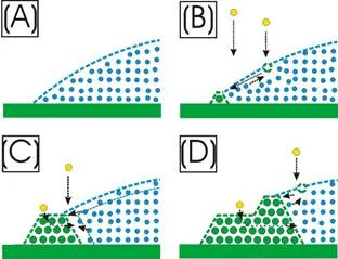
We explained the evolution kinetics of the stepped outer surface of the QD [68]. The summary of the kinetic is as follows. The intersection of the crystal surface with the droplet is the TPL, which serves as an initial place of crystallization [68]. When a Ga atom of the droplet meets an arsenic atom, they form a GaAs molecule. These GaAs species, making a Brown-like movement over the droplet surface, can reach the TPL, where the crystallization starts (Figure 6). The crystal seed at the TPL will grow on the account of further arriving arsenic species. The outer facet angle of the crystallization center at the edge will be the favorable 55° because it has enough time to find the optimal position (the low index facet). The crystallization seed grows partly upward and also partly in the direction of the droplet inside. During the process of solidification, a circular monocrystalline phase is formed at the droplet edge inheriting the orientation of the perfect substrate. During the process of solidification, the amount of Ga atoms in the droplets decreases so the droplet size decreases too. The outer side of the QD consists of steps of few MLs, where the front panel and the terrace of the step are (111) and (001) planes, respectively. It is known in fcc crystals that the surface energy of (111) facet is less than that of (001) facet; thus, the latter grows predominantly during crystallization. This takes place by the lateral shift of the low energy (111) step facets with the simultaneous areal growth of (001) facets. With the size decrease of the droplet, its edge moves inward, thus creating a new TPL or crystallization seed at the new place, and the whole process continues as before with the original droplet and substrate. The only difference is that the crystallization takes place along a circle of less and less diameter.
Ringlike QD preparation
GROWTH TECHNOLOGY OF RINGLIKE QD
The preparation process responsible for the DE formation of ringlike QDs is described in the case of GaAs nanostructures on AlGaAs (001) surface. The growth experiments are performed similarly as described in the previous section, but the technological parameters somewhat differs. On GaAs (001) wafers, first pure GaAs layer is grown, and it is followed by an AlGaAs layer with Al content of 0.3.Then the GaAs sample with AlGaAs layer must be cooled down to 300°C. On the surface, Ga is deposited as described in former section. Then θ = 3.75 ML gallium is deposited with the flux of 0.19 ML/s without any arsenic flux. During the annealing, the temperature remained the same (300 ºC), but the As pressure was 4 × 10⁻⁶ Torr. The production of the quantum objects was tracked continuously in the direction of [11¯1¯0] with the help of RHEED [67].Further, two types of ringlike nanostructures were generated with different amounts of deposited Ga. One of them was generated at 570°C on AlGaAs (001) surface applying 6.4 ML Ga. In this case, the AFM measurement shows ringlike QD with deep hole in the middle of the structure and very large clusters [95]. The other type of the nanostructures was prepared similarly, but the deposited Ga was less than that in the former case. The Ga coverage was 3.2 ML. In this case, the AFM picture shows special-shaped nanostructure with very deep crater in the middle surrounded by ringlike bulge formations and also sallow nanocraters, with plane rims (without bulge) [75, 76].
After the growth process, quantum objects are investigated using the AFM method, and the first mentioned types of nanostructure are studied with PL technique, too. Temperature-dependent PL spectra measured on the GaAs ringlike QD samples are compared with the conventionally shaped QDs.The technology can continuously be tracked by RHEED. The initial stage of the surfaces is the same as in the case of conventional QD. The RHEED pattern of the initial surface shows sharp streaks (stage t0on Figure 8). After the Ga deposition, the pattern diffuses on the RHEED screen similarly as in the case of QDs (stage t1). The deposited Ga is in liquid phase. The disappearance of the RHEED pattern originates from the appearance of the liquid phase of Ga droplet on the surface. However, after the Ga deposition, the change of the observed RHEED pattern is quite different. After the offering of arsenic background of 4 × 10⁻⁶ Torr, the RHEED pattern develops very slowly, over 5 min. Contrary to the case of conventionally shaped QDs, which is almost at the same time of the arsenic cell opening, the RHEED pattern changed suddenly. The developed pattern contains in the middle a streak with a small spot and around elongated larger spots. According the AFM measurement, the density of the ringlike structures is 1.5 × 109 cm–2. In this case, the effect of open surface on RHEED is larger than in the case of QD [69]. It is shown that the characteristic RHEED pattern of QD is still recognizable even if QD density is one order of magnitude less [43].
GEOMETRY AND ELECTRONIC STRUCTURE OF THE RINGLIKE QD
The shapes of ringlike QDs are various. The main parameters are the following: ring-middle diameter, width of the ring base, and height. As we will show, the facet angle is determined by the volume. The further shape parameter is the level of the ring middle. The ring middle can lie higher or deeper than the original substrate surface. At lower annealing temperature and at less arsenic ambient pressure, the droplet metamorphosis results in ringlike nanostructure with smaller crater in the middle [78–81]. For example, at 4.75 ML Ga deposition, under 1 × 10⁻⁵ Torr arsenic pressure and 350°C annealing for 10 min, the resulted structures are ring with shallow crater [79].In another case, if the ring center lies deeper [75, 77], the structure is called a nanohole. In this case, thermal etching is dominant. If the annealing temperature is higher and the arsenic ambient pressure is smaller, then we receive ring structure with low-lying center. For example, at 8 ML deposited Ga, at 520°C annealing and under various arsenic pressure, we can get nanostructures with various deepness in the middle. If the arsenic pressures are 3 × 10⁻⁶, 2 × 10⁻⁶, 1 × 10⁻⁶, and 1 × 10⁻⁷ Torr, then the holes are ca. 3, ca. 7, ca. 8.5, and 9.5 nm deep, respectively [62, 75, 76, 82]. The electronic structure is strongly governed by the shape of the nanostructure. Here, the advantages of the ringlike QD compared to the conventionally shaped QD are described using temperature-dependent PL spectra. Under measurement, the temperature ranges between 4 K and 300 K. The samples are excited by Ar+ ion laser at 488 nm wavelength. The resolution was better than 0.5 nm [83]. The PL spectra of the uncovered GaAs ringlike QD grown on AlGaAs surface are shown in Figure 9. At 4 K, the spectrum has five peaks. They can be explained as bound exciton (1.5129 eV), exciton bound to acceptor (1.4892 eV), and its longitudinal optical phonon replica (1.4577 eV). Further on at higher energies, two peaks appear (1.5308 and 1.5602 eV). The PL spectra were also recorded as a function of temperature. To verify the identification of the peaks, the temperature dependence of the band-gap energy of GaAs and that of the bound exciton were compared. At 4 K in the case of conventionally shaped QD with identical volume, three peaks can only be seen at lower energy range. It is visible that the quantum confinement in ringlike QD is larger than that in QD at same nanostructure volume. In the following, this phenomenon will be explained [83].
The base diameter of the QD (LQD) investigated is much larger, and its height (HQD) is also larger but comparable. Thus, here no quantum effects are expected. Therefore, it was impossible to detect a peak shift or peak broadening for QD. At the same volume, for ringlike structure, the laterally wide (LQR) nanostructure had a height (HQR) significantly less than 7 nm. Consequently, the supposition of quantum confinement produces proper result [83]. The PL spectra show characteristic peak width, depending on the temperature and the size distribution of these structures. At the same temperature, a broader size variation results in a broader PL peak. Under similar growth conditions, the PL peaks of ringlike structures have significantly narrower full width at half maximum (FWHM) (less than one third) than that of the conventionally shaped QDs [78, 84].The sharper PL peaks can be explained by follows. As it is known, both kinds of QDs is formed from a gallium droplet. Assume that the volume and its variation of the initial droplets are the same in both cases. The facet of the nanostructures is size dependent and cannot be arbitrarily sized [43]. For the QD, let’s start from the greater (111) facet (the approx. diameter (2r = LQD) is 100 nm [43]). For the ringlike QD, only the (113) facet can be taken into account because of the smaller volume (the approximate width (LQR) is 60 nm [43, 44, 83], dedicated to a circle segment). Due to the crystallographic constraints, the geometry of the formed QDs is determined. The height-to-diameter ratio cannot be arbitrary; it can be defined by a single parameter. If r (r = LQD/2) is the radius of the base circle belonging to the initial droplet, the volume of the developing QD, as a function of r, is given by V = 1.58r3. For the ringlike nanostructure, from the equality of the volumes, the w (w = LQR) parameter can be calculated as w = 0.71r. (This means that the nano-object with a parameter of 2r = 100 nm has (111) facets, and the other one with a parameter of w = 0.71 × 100 ~ 70 nm or less has (113) facets. It corresponds to the above presented measured data.) It means, that the height of the nanostructure influences commonly the quantum behavior. The heights of the QD and QR structures can be expressed as a function of their volumes: mQD = V1/3/1.34 and mQR = V1/3/6.56, respectively. Assuming the same variations of the volumes, it can be seen that the variation of the height for QR is much smaller than for QD; consequently, the corresponding FWHM of the PL peak is smaller [83].
SOME ASPECTS TO THE FORMATION OF RINGLIKE NANOSTRUCTURE
The primer information to discover the formation kinetic originates from RHEED tracking [67]. After the deposition of Ga on AlGaAs (001) surface, the RHEED picture is becoming diffused due to the amorphous nature of the phase present on the surface. The annealing phase begins after the offering of arsenic component (pAs = 4 × 10⁻⁶ Torr, Tsub = 300°C). After releasing the arsenic, some time is needed for the development of the characteristic sharp pattern, representative of the crystalline structure. This is an indication that the liquid state on the surface stays longer and that the material transfer processes helps the formation of the ringlike structures. For detailed technological parameters of the different DE nanostructures, we refer the readers to the literature [32–35, 43–45, 62].After the completion of the growth, the QR structures were investigated with AFM. The perspective AFM image and the top view with line scans are shown in Figure 10. The dimensions of QRs were determined from individual line scans. The density of the nanostructures determined from AFM pictures was 1.5 × 109 cm–2. It is visible that the middles of the nanostructures are deeper than the original surface level [85]. It can be shown, from the AFM measurement that although the shapes and sizes of QRs are fairly uniform, we can observe small deviations from these averages. It is often observed that the smaller diameter rings have deeper depressions in the center and the larger diameter rings have shallower ones in the middle. (In the illustrations, the smaller and larger objects are labeled with “S” and “L”, respectively.) The QRs have slightly elongated shapes due to the different binding properties in [110] and [11¯1¯0] directions [86].
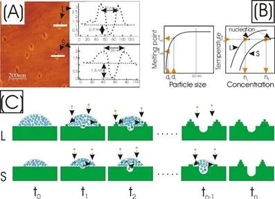
These facts are contradictory to the aspect ratios of ringlike QDs, and the explanation can help to understand the kinetics of the DE quantum structure formation. The explanation to this extraordinary behavior is as follows [85]. It is an obvious assumption that the larger droplets are leading to the development of rings of larger diameter and equally the smaller droplets to smaller rings. The intersection of the crystal surface with the droplet edge is the so-called TPL, which is the initial place of crystallization [85]. The TPL of larger diameter initiates a larger droplet, and equally, the smaller diameter forms from a smaller droplet. It is known from the liquid phase epitaxy that thermal etching takes place at the interface of the Ga melt and AlGaAs surface. This phenomenon was confirmed by analytical TEM for DE QD [69]. The Ga melt can solve the arsenide molecules (e.g., GaAs). These arsenide molecules originate partly from the thermal etching of the AlGaAs substrate surface and partly from the reaction of the external (from effusion source) arsenic atoms. (When a Ga atom of the droplet meets an arsenic atom from the environment, they form a GaAs molecule.) These molecules, due to thermal movement in the droplet, can reach the TPL, where the crystallization takes place. During the process of solidification, the material migrates from the middle to the edge of the nanostructure. A circular crystalline phase is formed at the droplet edge. The proposed kinetics for the formation is shown schematically in Figure 10. It is known that the melting point decreases with the reduction of the particle size. The normalized melting curve versus the diameter of the particle (Figure 10) shows that when the particle size is less than 50 nm, then the melting point depends very strongly on size. In the nanorange, this dependence on the size is stronger than for the bulk. What makes it more complicated is the fact that the melting point depends on the particle shape as well. In this case, the Ga droplet’s shape is a segment of a sphere. Its width in the middle falls in the range of 10–20 nm. Here, the change in the melting point is particularly sharp [85]. Around the edges the structure is thin. The experimentally obtained melting curves for near spherical metal nanoparticles show similarly. We use these curves for the qualitative assessment. This indicates that the melting point of the large and that of the small Ga droplets can differ considerably. The solubility curves for different particle sizes (Figure 10) show that at the same temperature, the larger droplet has lower saturating concentration than the smaller one. The meaning of this is that crystallization in the larger droplet will take place earlier, at lower arsenide concentration than in a smaller one. The smaller droplet will crystallize later, during arsenide concentration.
The temporal evaluation of the smaller and larger ringlike QDs is shown in lower part of the figure onset (Figure 10) [85]. In other words, in the larger droplets, the probability of the formation of the crystallization seeds is higher; therefore, the crystallization takes place earlier so less time is spent on material transportation, causing the development of the depression in the middle. When the droplets are small, the probability is less, and crystallization starts later, leaving more time for the formation of deeper depression in the center of the ring. This process is influenced by other factors as well. The melting temperature of the nanostructure is dropping with its diminishing size, staying longer in liquid state at the same temperature, spending more time on the formation of deeper in the center [85]. The above-described finding can be proven by further experiments (in Section 5.1, ringlike nanostructure production is described where the amounts of the deposited Ga were 3.2 and 6.4 ML, respectively). The explanation is as follows [85, 87, 88]: At a given temperature, there is a critical droplet size (CDS) under which the solution begins. After the Ga deposition, droplets form, followed by the growth of the larger droplets at the expense of smaller ones according the Ostwald ripening. When the droplet is smaller than the CDS, the substrate solution begins. In the case of Ga 6.4 ML, the formation of small holes and large clusters can be observed. The sizes of the droplets formed are above the CDS. After the deposition, the differentiation of the droplets begins. The smaller droplets reach critical size and start solving the substrate. This state is frozen via opening the arsenic cell. When the deposited Ga is 3.2 ML, we can observe shallow holes with plane rims. The explanation is as follows [85, 87, 88]. In this case, the quantity of the deposited Ga is small. The formed droplets are under CDS. Therefore, the solution starts under the droplets immediately after the droplet formation. Under the small droplets, the solution is faster, but the material of liquid Ga is used up in a short time. The reduction in material is due to, first, the solution and, second, the migration of materials toward the larger droplets. After a short time, at the smaller droplets, the solution stops, while it carriers on further under the larger ones. The larger droplets will not be spent, and therefore the surrounding ring will freeze after the opening of the arsenic cell.
Specular-shaped QDs and complexes
THE INVERTED QDS
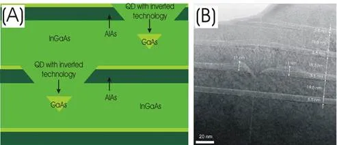
The ringlike QD is an unconventional QD, which has advantages over the conventional QD. As we have shown, the DE technique is a many-sided tool in this field. It allows us to fabricate further interesting nanostructures. Here, we will further discuss unconventional-shaped QDs and their complexes. In the present subsection, we will focus on an alternative QD preparation technique. This is not only an alternative preparation but the QD with inverted technology can also have advantages at special application?n.A further recent method for the fabrication of strain-free QD is the nanohole filling. The nanohole is created by localized thermal etching, and it is filled subsequently [95]. This is a QD with inverted technology. The localized thermal etching takes place at conventional MBE growth temperatures, and we expect only very low level of crystal defects. The nanoholes are created in a self-organized fashion by local material removal [89]. For the inverted QD fabrication, nanoholes are generated using Al droplets on AlAs surface. Subsequently, the holes are filled with GaAs layer to form QDs of controlled height [ 90]. The nanoholes are filled with GaAs in pulsed mode.
Here, we show a cross-sectional study of an inverted QD [66]. The technology of this QD is as follows. The structure is grown on GaAs (001) surface. On the surface, AlGaAs and AlAs layer sequence is grown. The AlGaAs layer has 0.23 Al content. The AlAs and the AlGaAs layers are 5.5 and 19.5 nm, respectively. After the growth of every AlAs layer, 3.2 ML Al is deposited at 650°C without any arsenic flux. The deposited Al MLs form droplets on the surface. This is followed by an annealing step of 180 s, during which the droplets transform into nanoholes.
Following that, the holes are partially filled by the deposition of 0.6 nm thick GaAs in a growth-interrupted fashion. During the hole filling, the substrate temperature is 600°C. Depending on the foreseen high of the QD, some growth of 0.5 s and pause of 30 s sequences are carried out. Finally, the GaAs QD can be covered with AlGaAs. The scheme and the TEM image of the inverted QD structure are shown in Figure 11. The above-described pulsed technique allows us to create not only single QDs but also vertically aligned QD pairs [91]. The distances on the TEM image correspond with the intended layer thicknesses. The picture shows GaAs QD embedded in AlGaAs barrier material. Furthermore, the TEM image shows a thickening of the AlAs layer in the surrounding the nanohole. Elementary maps taken using electron energy loss spectroscopy confirm that the thickened region consists of AlAs. We identify the additional AlAs on top of the flat AlAs layer as the wall that surrounds the nanohole opening. Furthermore, the TEM image on Figure 11 shows that the next AlAs layer grown on top of the inverted QD layer is bended upward at the location of the QD, resulting in the formation of a kind of hill [66].
THE LATERALLY ALIGNED QD PAIRS
Two semiconductor QDs in close proximity, which can each spatially confine an individual charge carrier in a discrete energy level, interact quantum mechanically with each other. In particular, the wave functions of the charge carriers confined in each QDs of the pair begin to overlap, resulting in an efficient tunneling. Furthermore, the wave functions may become mixed to develop molecular orbital. Moreover, resonance in the optical range leads to the formation coupled QD pairs with the help of dipole–dipole interaction. These research leads toward quantum information processing. The QD pairs and their systems offer, at least conceptually, the potential of implementing scalable arrays of qubits. In this part, we are dealing GaAs QD pairs prepared on AlGaAs surface with the usage of the anisotropy of the (001) oriented surface. We will show two preparational series. One of them is carried out under lower temperature, at less amount of deposited MLs. The other ones is prepared under higher temperature at higher amount of deposited Ga.
In the first case, AlGaAs with Al content of 0.27 is grown on the GaAs (001) surface. After this, Ga droplets are created at 330°C temperature on the substrate. The crystallization happens at 200°C, under accurate control of the arsenic flux [104]. The ripened structure basically consists of two QDs aligned in the [0 1¯1¯ 1] crystalographic direction. The average base size and height of each QD are 45 and 10 nm, respectively. The QDs are separated by an average distance of 39 nm between their apexes, as measured by AFM. The density of the structure is 2 × 108 cm–2 [104]. For the study of its optical properties, the QD pairs are embedded in AlGaAs barrier layer. The second technology is carried out on GaAs surface. First, AlGaAs layer is grown with 0.3 Al amount. At 550°C substrate temperature, a large amount of Ga is deposited to create droplets on the surface. The structure is “arsenized” by fine control of the flux [99]. The resulting dots are rather large. The individual pairs have an interdot distance of about 130 nm and are aligned along the [0 1¯1¯ 1] direction. The dots with a height of 10 nm reside on a shallow base with a diameter of 300 nm. The density of the structure is 2.3 × 108 cm–2 [99]. For optical characterization, the QD pairs are buried by the deposition of AlGaAs layer.
In the first case, the micro-PL spectra of a single QD pair show the ensemble of emissions, which may indicate the existence of a tunnel coupling between the members of the pair. However, it must be mentioned that these emission lines are still not fully understood [104]. At the second experiment, the PL study is performed at a rather larger inter-dot separation. Here the formation of coherently coupled molecular QD states is suppressed, and excitonic interactions between neighboring QDs within each members are weak [105]. The process of the QD pair evolution is also not fully understood. Instead of the hemispherical shape of the initial droplet, the ripened structure is anisotropic. The explanation is based on the anisotropic surface potential of the GaAs (001) surface (Figure 12).
CONFIGURATION OF QD ENSEMBLES
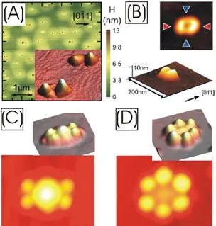
Until now, the most widely studied system of interacting self-assembled QDs is a vertically stacked QD molecule. However, this system is limited by its one-dimensional nature and is not easily scalable. Alternatively, a variety of techniques can be used to modify the substrate to nucleate laterally coupled QD molecules in two dimensions by MBE technology. Various shape droplets can subsequently serve as templates for further growth, without the need for further surface preparation.The DE-like created nanohole and also the homo-DE-grown island can serve as an initialization place for the growth of further nanostructures. The nanohole as a template for QD molecules is demonstrated by Songmuang and coworkers [106]. The nanohole can serve as a template for QD pair too [107]. Salamo and coworkers proposed a new way for the preparation of QD molecules [92-94, 110]. They adopt a hybrid growth approach, utilizing both DE and strain-induced growth to overcome some limitations of the Stranski–Krastanov QD growth mode alone on a planar GaAs surface [102]. Using MBE, a self-assembled InGaAs QD molecule is realized around GaAs mound formed by DE on GaAs (001) surface [102].
The number of QDs per GaAs mound can be effectively controlled by varying the InAs ML coverage. The number of QDs per template ranges from two to six. The technology is as follows. On GaAs (001) surface, 3 ML Ga is deposited at 500°C without any arsenic flux to form Ga droplets. Subsequently, 80 s of annealing occurs, and the substrate temperature is decreased to 150°C. The Ga droplet is crystallized under 1.3 × 10⁻⁵ Torr equivalent pressure for 100 s. During this time, nanoscale GaAs mound forms as template. The substrate temperature is raised again to 500°C, and InAs deposition follows. If the deposited InAs are 1.4, 1.6, and 2.0 ML, then the created nanostructures are bi-QD molecule, quad-QD molecule, and hexa-QD molecule [108]. During the QD molecule preparation, the height of the GaAs mound decreases from the original value, and also the diameter decreases. It appears that the InAs growth started mixing with the Ga atoms from the GaAs mounds, resulting in InGaAs shoulders on initial templates. This technique allows to fabricate the so-called quantum-rod pair and lip-shaped structures too [108]. The technology is extended with incident angle-controlled molecular beam technique [109].
