Introduction
Careful investigations of the structural, refractive, conductive, and wetting properties of the innovative hybrid materials modified with effective nano- and bio-objects are timely and quite popular [1–6] because of the relevance study of new physical and chemical effects in them. Structured inorganic and organic materials, including liquid crystal ones, are able to optimize the technological processes for nano- and bio-technologies, as well as to extend the possible their application for the purposes of telecommunications, display, laser, biomedical engineering, industrial production, etc.
It should be said that the study of the structural and optical effects in the materials has a special place in the development of modern innovative technologies. This is due to the substantial increase in applications last, as the photon energy lies in the range of electronic and vibrational transitions in matter, and therefore, this circumstance allows the use of light and more particularly laser radiation, to obtain unique information about structural and dynamic refractive properties of the materials. Moreover, it permits to manifest new and classic confirmation of the effects in them and to use laser sources for modeling properties of the investigated matrix systems.
This chapter partially summarizes the prospects of the process of surface structuring (e.g., some inorganic materials) and the volume (e.g., some organic systems) in order to create and advocate new composites with unique improved their physical and chemical properties.
FEATURES OF STRUCTURATION OF THE SURFACE OF INORGANIC MODEL MATERIALS
Covalent bonding of the CNTs, as an indicator of enlightenment, the strengthening of materials, changing their resistance and laser strength.
Among other perspective nanoparticles and nanostructures, the carbon nanotubes (CNTs) occupy the special place. The basic features of carbon nanotubes are regarded to their branched surface, high conductivity, strong hardness of their C–C bonds, little value of the refractive index as well as to their complicated, and unique mechanisms of charge carrier moving [7–10]. These characteristics permit to apply the CNTs materials with good advantage in order to improve the physical and chemical properties of the inorganic systems especially when the CNTs have been deposited on the material surfaces.
It should be mentioned that to modify the properties of the inorganic materials via their surface treatment, the SWCNTs type #704121 with the diameter placed in the range of 0.7–1.1 nm purchased from Aldrich Co. has been used. These nanotubes have been deposited on the material surface using IR CO2‐laser with p‐polarized irradiation at wavelength of 10.6 μm and power of 30 W. Moreover, CNTs have been placed at the materials interface under the conditions when an additional electric field of 100–600 V cm−1 has been applied in order to orient the nanotubes in the vertical position during the deposition process. This procedure has been partially shown in the RU patents [11, 12]. The spectra of the nanotubes‐treated materials have been obtained using Perkin‐Elmer Lambda 9 and Furrier FSM‐1202 instruments as well as using VIS SF‐26 device operated in the range of 250–1200 nm. Surface mechanical hardness has been revealed using the CM‐55 instrument as well as via using of the micro‐hardness device PMT‐3M (produced by “LOMO”, Saint‐Petersburg, Russia) with the ability to vary an indenter forces. The laser strength has been checked with pulsed nanosecond Nd‐laser. The special accent has been given to observe the relief at the material surface via checking the wetting angle. In this case, the camera with parameters as Compact F1.6 1/3 CS Mount 6.0–60 mm Manual Focal Iris Zoom Lens for CCTV Camera (Black) has been applied. The modified surface analysis has been made using Solver Next AFM (purchased from NT MDT Co., Zelenograd, Moscow region, Russia).
ITO CONDUCTING LAYER: SPECTRAL PARAMETERS, WETTING PHENOMENON, LASER AND MECHANICAL CHARACTERISTICS
It should be mentioned that an emphasis has been given on the ITO‐conducting layers modification due to the reason that these structures have so broad area of the application in the general telecommunication systems, solar energy area, and biomedicine as well as in display, gas storage and laser technique [13–20]. For example, if one of the optoelectronic key element, such as electrically or light‐addressed spatial light modulators (SLMs) can be considered, it should be said that besides of the solution to obtain the high resistivity and good speed, some other important problem should be resolved. It connected with the possible increase of the transparency, mechanical and laser strength of the SLM elements as well. Thus, nanostructuration process permits to find new ways to resolve the problem mentioned above with good advantage. In this case, the influence of the surface treatment procedure on the materials basic characteristics can be taken into account.
The data showed in Figures 1 and 2 as well as in Tables 1 and 2 support the spectral evidences, the mechanical properties, the laser features, the resistance values, and the wetting angles. It should be mentioned that an additional surface electromagnetic wave (SEW) treatment has been made to modify the ITO relief in order to decrease the roughness and resistivity as well as to apply one as an orienting coating for the classical nematic liquid crystal cells [21, 22].

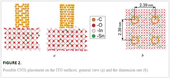

One can see from Figure 1 data that the structuration of the ITO surfaces with oriented CNTs provokes the shift of the spectral parameters (a) and increase the transparency (b). The molecular dynamics method based on the LAMMPS program [23, 24] has been made to support these results. Data of this simulation have supported the bonding existing effect and testified that the one has been coincided with the diameter and speed of the CNTs under the laser‐oriented deposition (LOD) conditions. The data presented in Figure 2 show the possible bonding between carbon atoms and atomic surface layer.
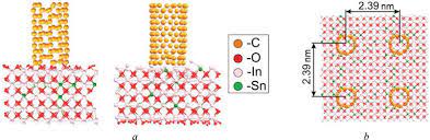
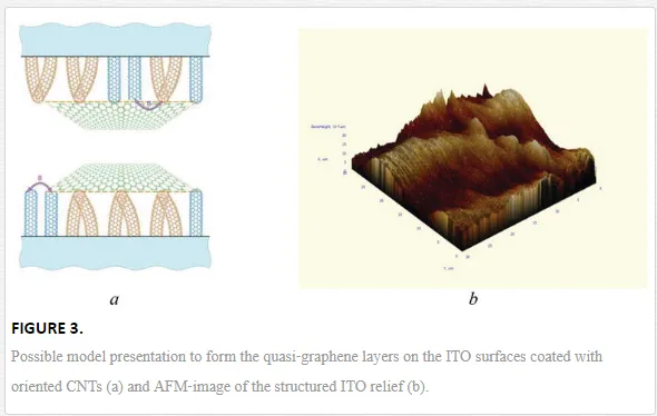
It should be mentioned that this ITO surface modification reveled by LOD has provoked the dramatically decrease of the resistivity. It can be explained by the formation of the possible quasi‐graphene layer due to the fact that CNTs reveal the large charge carrier moving from the core of the nanotubes and show the donor acceptor properties too. Figure 3a presented the tentative model picture to form the quasi‐graphene layers on the ITO surfaces structured by LOD. As an additional, the AFM‐image is shown in Figure 3b in order to present the real structured optimized relief.
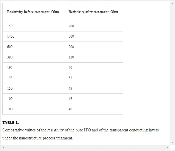
To observe the change of the resistivity, one can see Table 1 data. Thus, the resistivity parameters can be change up to 2–3 times. It can be important for the future design of the telecommunication systems, such as light‐addressed and electrically addressed SLMs, electrically controlled display and holographic elements, etc., because it should provoke the essential decrease of the applied voltage. Indeed, the data presented in Table 1 have been obtained for the initial different pure ITO coatings with different their thickness and treated at different annealing temperatures.
Among these advantages, the mechanical hardness and laser strength improvement have been shown as well. The data of Table 2 support this fact. It should be testified that the mechanical hardness and laser strength of the ITO‐conducting layer can be successfully increased via CNTs treatment. It should be mentioned that traditionally the HfO2 coatings have been deposited on the ITO surface to eliminate their roughness and increase the strength, but the CNTs modification can provoke the better results via applying the LOD technique.
Some evidences to increase the wetting angle have been obtained too for the ITO relief studied. Thus, the pure ITO coatings additionally treated with the surface electromagnetic waves have revealed the wetting angle close to 70–75°. After nanostructuration process using LOD technique, the wetting angle has been increased and placed in the range of 85–89°.
Analyzing these evidences, it should be noticed that the ITO‐relief obtained can be sufficiently used especially in the display and SLM technique due to the fact that the modified relief at the ITO surfaces can be considered as the conducting layer with the decreased resistivity as well as the orienting one to align the LC dipoles with good advantage. Moreover, these structured ITO can be prospectively using in the solar energy area and in the biomedicine as well as in the general optoelectronics too especially due to their increased transparency.
MGF2 AND RELATIVE STRUCTURES: SPECTRAL PARAMETERS, WETTING PHENOMENON, AND MECHANICAL HARDNESS
Using the mentioned above designed laser technologies based on the oriented deposition of the carbon nanotubes [11, 12] on the surface of optical materials including as well MgF2, CaF2, BaF2, LiF, NaCl, KBr, KCl, etc. materials operated in the UV and in the IR spectral range, the study of the spectrum of transmittance, micro‐hardness, changing the ability to water absorption, etc. is important. Results for the obtained transmittance and the reflection spectra of the group of randomly selected samples are shown in Figure 4. One can observe the essential change of the spectral characteristics for the 200–500 nm and for the near‐IR spectral range. Moreover, for the BaF2 structures, the reflection spectrum change has been obtained up to 16 micrometers.
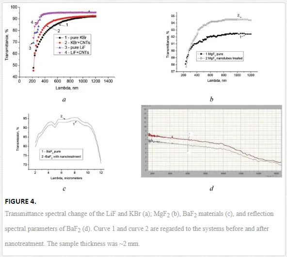
Analyzing these data, it is evident that the process of laser deposition of CNTs on the surface of the studied materials changes the spectral parameters, leading to a substantial increase of transmittance and decrease of Fresnel losses due to the covalent binding of the CNTs to the surface of the material [25, 26] with regard to the small value of the imaginary part of permittivity of CNTs and their small refractive index that can be <1.1.
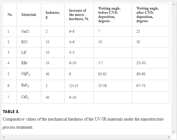
Moreover, dramatically change of the micro‐hardness and the wetting angle has been obtained for these systems. The comparative data before and after laser deposition of the CNTs are shown in Table 3. Thus, micro‐hardness can be increased more than 6–10%, and the angle of wettability can be changed from 1.5 to 5 times. Of course, not only essential mechanical properties of carbon nanotubes should be considered when one analyzes these data, but also the formation of predicted covalent bonds between carbon nanotubes and the surface atoms of the investigated materials. It should be mentioned that the analytical calculations presented in the paper [26] for the model MgF2 structure have shown that in order to destroy the structured material surface we should firstly to bend the vertically oriented nanotubes with energy of 1.8 × 10⁻²⁰ J, which is in five times larger than the one, which can be applied to simply remove the nanotubes from the surface after destroying MgC bonding. This simple model can be used to explain the results of the dramatic increase of mechanical surface hardness of MgF2 covered with nanotubes placed by LOD technique.
Analyzing these evidences, one can propose that some hydrophilic properties of the functional UV‐IR materials can be changed to reveal the hydrophobic features. That is very important in the Fourier spectrometry devices, for the microscopy area, as well as for the biomedicine. For example, the output windows of magnesium fluoride are used in the lamps for quartz treatment of medical institutions. It also can be required for the some substrate of the spatial light modulators which area of their operation should be extended to the UV and IR spectral ranges.
In addition, registered increase of the spectral characteristics, macro‐hardness parameters and of the wetting phenomena too indicates the novel tendency to find unique way to improve the technical parameters of these materials under the condition of the oriented CNTs laser deposition technique for the purpose of the general optoelectronics, solar energy, and biomedicine systems.
METAL AND SEMICONDUCTOR MATERIALS: SPECTRAL PARAMETERS, WETTING PHENOMENON, AND MECHANICAL HARDNESS
Some materials from the metal and semiconductor groups have been studied in order to accept the knowledge about the influence of the nanostructuration process on the basic physical parameters of this type of the materials. Partially, the data are presented in Figure 5. It should be noticed that in the case of the analysis of the spectra, one took into account the change of the spectrum with one‐sided processing of the material and processing from two their sides.

The micro‐hardness results reveal the increase of these parameters too. Thus, for the Al, Cu, ZnS, ZnSe materials, the micro‐hardness has been increased up to 7, 9, 5, 5%, respectively. It should be mentioned that the indenter with the forces of 30 and 20 g has been used to treat the metal and semiconductor materials, respectively.
The molecular dynamics method has supported the results of the spectral and the mechanical properties changing due to the incorporation of the CNTs into the materials surfaces and due to form the possible bonding between the carbon atom and the original material surface atoms of Al and ZnS materials. It should be mentioned that the penetration depth has been depended on the velocity of the CNTs and their diameters. The molecular dynamics results are shown in Figure 6. This analysis has been made using the procedure in the framework of the LAMMPS program [23, 24].


It should be noticed that the interaction between Zn and S atoms in the penetration process of CNT into Zn‐S surface was described using Tersoff many‐body potential in which parameters are given in publication [27]. Interaction between Al atoms was described using embedded atom method (EAM) [28] parametrized according to Ref. [29].
To describe the interaction between CNT and Al substrate, the 12–6 potential E=4ε[(σr)12−(σr)6]E=4ε[(σr)12−(σr)6]has been used. The interaction parameters were fit as: ε = 2.63 eV, σ = 1.91 Å based on interlayer distance between graphene and Al surface. To describe the interaction between CNT and Zn atoms of the substrate, the parameters for 12–6 potential were fitted as ε = 0.011 eV, σ = 1.80 Å. Interaction between C and S was taken two times smaller than for Zn‐C. The interaction between carbon atoms in the CNT was described using Tersoff many‐body potentials with parameters described in Ref. [23].
The molecular dynamics simulations have been carried out at constant temperature about 300 K. The total time of simulation has been of 60 ps with the time step of 1 fs. The velocities of the tubes have been varied from 100 to 600 m×s−1 according to the experiments.
Thus, using the consideration based on the ITO, MgF2 and relative structures, Al, Cu, ZnS and ZnSe materials, the current study can propose the CNTs laser treatment as the innovative way to modify the important physical and chemical characteristics of these inorganic materials.
Analyzing these evidences, one can remember that Al is the material used to fabricate the aviation, aerospace, food processing and the production of tableware; copper is a material for the manufacture of wires for electrical industry; ZnS and ZnSe are the materials for the manufacture of space components and devices of technical sensors, etc. Thus, all of the mentioned above area of the application of the materials under the consideration can be essentially exceeded via using the LOD technique with good advantage.
Features of the structuring of the volume of model polymers and liquid crystals: change of the refractive parameters as indicator of the changes of the photoconductive, spectral and structural properties
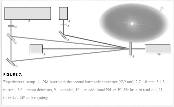
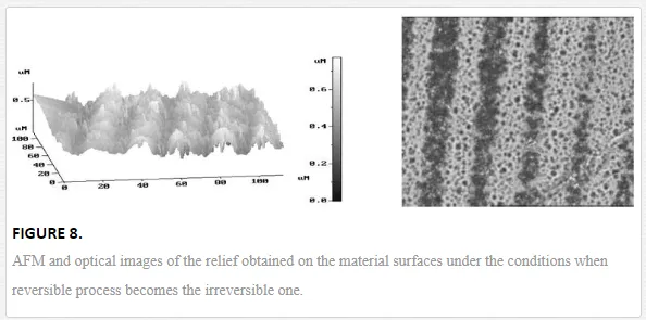
Using four‐wave mixing of laser beams (see Figure 7) in the nanosecond range of durations, at the wavelength of the second harmonic of a neodymium laser λ = 532 nm, with variation, as energy density or spatial frequency λ, the investigation of the change of refractive properties of a large group of conjugated organic materials by recording the diffraction efficiency in the diffraction Raman‐Nath has been made. The scheme and the conditions are coincided to that considered before in the papers [14, 30]. It should be mentioned that for all materials studied, the threshold value of the input energy density at which the reversible process has been transfer to the irreversible one has been detected. Some AFM‐image is shown in Figure 8, which corresponded to thermal replica on the material surface to indicate this fact. One can see that the spatial frequency approximately equaled to 90–100 mm−1 has been formed.
The values of light‐induced additives to the refractive index have been calculated, and the range of variation of cubic nonlinearity and nonlinear refraction has been defined. It is established that these values are comparable with those obtained for three‐dimensional silicon structures. But, it should be noticed that the technology of obtaining thin films of conjugated organic materials significantly easier and their thickness is an order of magnitude less. The main results of the largest light‐induced change of the refractive index Δni in a number of structured organic materials, for example, polyimide PI, 2‐cyclooctylamino‐5‐nitropyridine (COANP) and nematic liquid crystals (NLC) with different concentrations of the sensitizers and treated at different energy densities are systematic and presented in the comparative Table 4.
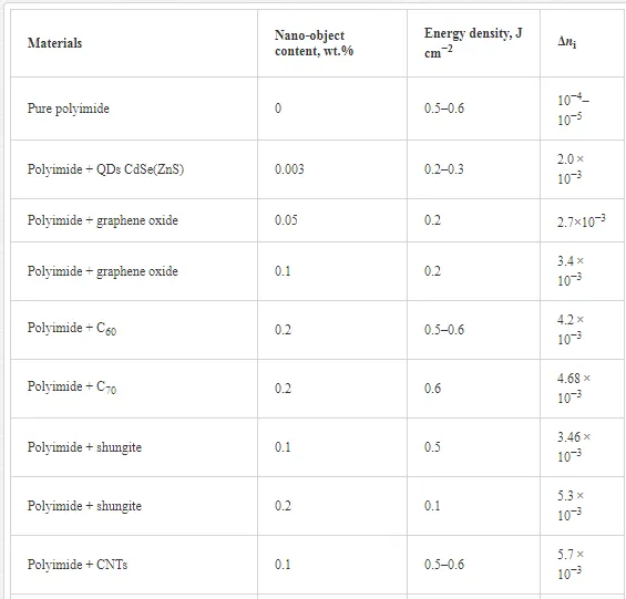

As nano‐ and bio‐sensitizers the fullerenes, shungites, carbon nanotubes (CNT), quantum dots (QD), oxides graphene, DNA has been used. The explanation of the change of the refractive properties of the organic conjugated systems with structuring volume of the medium is given in the framework of the significant growth of the polarizability, dipole moment, and the way of the transfer of charge carriers from intramolecular electron donor is not on the intramolecular acceptor but to the intermolecular acceptor with high electron affinity and ability to delocalize of not one, but a larger number of carriers [31, 32]. Qualitative picture is shown in Figure 9.

Analyzing the basic experimental data presented in Table 4, it should be remembered that the different types of the sensitizers, their content, and energy density have been applied. Moreover, the experiments have been performed at the close spatial frequencies and at the same laser pulse width. One can see that the values of the laser‐induced refractive index have been exceeded the ones obtained for the chosen pure matrix systems. It should be mentioned that the refractive features have been connected with the increase of the charge carrier mobility obtained via photoconductive experiments. The comparative analysis to check the increase of the charge carrier mobility has been made via procedure shown in the paper [33].
It should be said that the calculated values of nonlinear refraction n2 and third‐order nonlinear susceptibility χ(3) are included in a range of values: n2 = 10−10–10−9 cm2×W−1 и χ(3) = 10−10–10−9 cm3×erg−1 [30, 31, 34–36]. The growth of refractive coefficients correlated with the change of the photoconductive (increase of mobility of charge carriers), and it is connected with the changes in the order parameter of the studied materials and with the infrared shift of their spectral characteristics. It has been registered to the photosensitivity and has been calculated via checking the charge carrier mobility. Moreover, the tendency of the change of the nano‐doping to bio‐doping one has been discussed because the bio‐doped organics have shown the same refractive parameters change [37, 38]. The correlations indicated above can be used, on the one hand, for the basis of the predicted paths to extend the use of organic conjugated structured materials for the industrial and the biomedical applications, on the other hand, for the assessing of the ability of the competing influence of bio‐objects, in comparison with nano‐objects, due to nontoxicity and easy renewability from the World Ocean these biological structures.
Conclusion
Analyzing the obtained and discussed data, it should be concluded the followings:
1. Structuration of the inorganic material surfaces (based, e.g., on the ITO structures, MgF2 and relative systems, Al, Cu, ZnS and Znse ones) has predicted the spectral, mechanical and wetting features change. The increase of the transparency, hardness, and wetting angle has been revealed.
2. Structuration of the inorganic material surfaces based on ITO has shown and supported the essential decrease of the resistivity. It can provoke the decrease of the applied voltage when these ITO coatings are considered as the transparent conducting layers in the spatial light modulators and in the related devices.
3. Structuration of the inorganic material surfaces based on ITO via CNTs‐oriented laser deposition technique can provoke to form the possible quasi‐graphene layers, which can easy explain the change of the ITO resistivity due to large charge from the core of the CNTs and their donor‐acceptor properties.
4. Doping of the organic materials by studied nanoparticles has revealed the drastically change of the laser‐induced refractive index that is larger than the ones obtained for the pure organic conjugated matrixes.
5. Calculated refractive parameters of the nanoparticles doped organics can be compared with the analogous refractive parameters obtained for the classical inorganic bulk crystals.
6. The laser‐induced change of the refractive index of the nano‐doped organics can be compared with the analogous refractive parameters obtained for the bio‐doped organics materials based, for example, on the liquid crystal ones.
7. Applications of the materials, which body and interface can be modified with effective nanoparticles, can be extended essentially. The solar energy, gas storage systems, information technology, displays, and the biomedicine can accumulate the knowledge and the practical results